SLLSEN8C September 2015 – June 2017 TL16C752D
PRODUCTION DATA.
- 1 Features
- 2 Applications
- 3 Description
- 4 Revision History
- 5 Description (continued)
- 6 Pin Configurations and Function
- 7 Specifications
-
8 Detailed Description
- 8.1 Overview
- 8.2 Functional Block Diagrams
- 8.3
Feature Description
- 8.3.1
Functional Description
- 8.3.1.1 Trigger Levels
- 8.3.1.2 Hardware Flow Control
- 8.3.1.3 Auto-RTS
- 8.3.1.4 Auto-CTS
- 8.3.1.5 Software Flow Control
- 8.3.1.6 Software Flow Control Example
- 8.3.1.7 Reset
- 8.3.1.8 Interrupts
- 8.3.1.9 Interrupt Mode Operation
- 8.3.1.10 Polled Mode Operation
- 8.3.1.11 Break and Timeout Conditions
- 8.3.1.12 Programmable Baud Rate Generator
- 8.3.1
Functional Description
- 8.4 Device Functional Modes
- 8.5
Register Maps
- 8.5.1 Principals of Operation
- 8.5.2 Receiver Holding Register (RHR)
- 8.5.3 Transmit Holding Register (THR)
- 8.5.4 FIFO Control Register (FCR)
- 8.5.5 Line Control Register (LCR)
- 8.5.6 Line Status Register (LSR)
- 8.5.7 Modem Control Register (MCR)
- 8.5.8 Modem Status Register (MSR)
- 8.5.9 Interrupt Enable Register (IER)
- 8.5.10 Interrupt Identification Register (IIR)
- 8.5.11 Enhanced Feature Register (EFR)
- 8.5.12 Divisor Latches (DLL, DLH)
- 8.5.13 Transmission Control Register (TCR)
- 8.5.14 Trigger Level Register (TLR)
- 8.5.15 FIFO Ready Register
- 8.5.16 Alternate Function Register (AFR)
- 8.5.17 RS-485 Mode
- 8.5.18 IrDA Overview
- 8.5.19 IrDA Encoder Function
- 9 Application and Implementation
- 10Power Supply Recommendations
- 11Layout
- 12Device and Documentation Support
- 13Mechanical, Packaging, and Orderable Information
8 Detailed Description
8.1 Overview
The TL16C752D UART is pin-compatible with the ST16C2550 UART in the PFB package. It provides more enhanced features. All additional features are provided through a special enhanced feature register.
The TL16C752D UART will perform serial-to-parallel conversion on data characters received from peripheral devices or modems and parallel-to-parallel conversion on data characters transmitted by the processor. The complete status of each channel of the TL16C752D UART can be read at any time during functional operation by the processor.
Each UART transmits data sent to it from the peripheral 8-bit bus on the TX signal and receives characters on the RX signal. Characters can be programmed to be 5, 6, 7, or 8 bits. The UART has a 64-byte receive FIFO and transmit FIFO and can be programmed to interrupt at different trigger levels. The UART generates its own desired baud rate based upon a programmable divisor and its input clock. It can transmit even, odd, or no parity and 1-, 1.5-, or 2-stop bits. The receiver can detect break, idle or framing errors, FIFO overflow, and parity errors. The transmitter can detect FIFO underflow. The UART also contains a software interface for modem control operations, and software flow control and hardware flow control capabilities.
8.2 Functional Block Diagrams
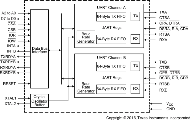 Figure 14. TL16C752D Functional Block Diagram
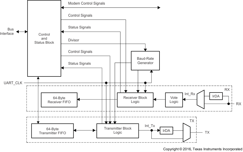
NOTE:
The vote logic determines whether the RX data is a logic 1 or 0. It takes three samples of the RX line and uses a majority vote to determine the logic level received. The vote logic operates on all bits received.8.3 Feature Description
8.3.1 Functional Description
The TL16C752D UART can be placed in an alternate mode (FIFO mode) relieving the processor of excessive software overhead by buffering received and transmitted characters. Both the receiver and transmitter FIFOs can store up to 64 bytes (including three additional bits of error status per byte for the receiver FIFO) and have selectable or programmable trigger levels. Primary outputs RXRDY and TXRDY allow signaling of DMA transfers.
The TL16C752D UART has selectable hardware flow control and software flow control. Both schemes significantly reduce software overhead and increase system efficiency by automatically controlling serial data flow. Hardware flow control uses the RTS output and CTS input signals. Software flow control uses programmable Xon and Xoff characters.
The TL16C752D device includes a programmable baud rate generator that can divide the timing reference clock by a divisor between 1 and 65535. A bit (MCR7) can be used to invoke a prescaler (divide by 4) off the reference clock, prior to the baud rate generator input. The divide by 4 prescaler is selected when MCR7 is set to 1.
8.3.1.1 Trigger Levels
The TL16C752D UART provides independent selectable and programmable trigger levels for both receiver and transmitter DMA and interrupt generation. After reset, both transmitter and receiver FIFOs are disabled and so, in effect, the trigger level is the default value of one byte. The selectable trigger levels are available through the FCR. The programmable trigger levels are available through the TLR.
8.3.1.2 Hardware Flow Control
Hardware flow control is composed of auto-CTS and auto-RTS. Auto-CTS and auto-RTS can be enabled or disabled independently by programming EFR[7:6].
With auto-CTS, CTS must be active before the UART can transmit data. Auto-RTS only activates the RTS output when there is enough room in the FIFO to receive data and deactivates the RTS output when the RX FIFO is sufficiently full. The HALT and RESTORE trigger levels in the TCR determine the levels at which RTS is activated or deactivated. If both auto-CTS and auto-RTS are enabled, when RTS is connected to CTS, data transmission does not occur unless the receiver FIFO has empty space. Thus, overrun errors are eliminated during hardware flow control. If not enabled, overrun errors occur if the transmit data rate exceeds the receive FIFO servicing latency.
8.3.1.3 Auto-RTS
Auto-RTS data flow control originates in the receiver block (see Figure 14). Figure 16 shows RTS functional timing. The receiver FIFO trigger levels used in Auto-RTS are stored in the TCR. RTS is active if the RX FIFO level is below the HALT trigger level in TCR[3:0]. When the receiver FIFO HALT trigger level is reached, RTS is deasserted. The sending device (for example, another UART) may send an additional byte after the trigger level is reached (assuming the sending UART has another byte to send) because it may not recognize the deassertion of RTS until it has begun sending the additional byte. RTS is automatically reasserted once the receiver FIFO reaches the RESUME trigger level programmed via TCR[7:4]. This reassertion allows the sending device to resume transmission.

8.3.1.4 Auto-CTS
The transmitter circuitry checks CTS before sending the next data byte. When CTS is active, the transmitter sends the next byte. To stop the transmitter from sending the following byte, CTS must be deasserted before the middle of the last stop bit that is currently being sent. The auto-CTS function reduces interrupts to the host system. When flow control is enabled, the CTS state changes and need not trigger host interrupts because the device automatically controls its own transmitter. Without auto-CTS, the transmitter sends any data present in the transmit FIFO and a receiver overrun error can result. Figure 17 shows CTS functional timing, and Figure 18 shows an example of autoflow control.

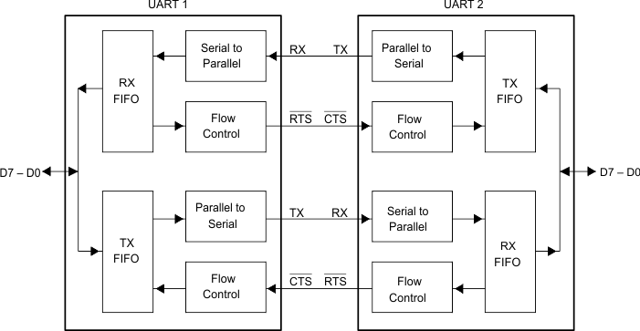 Figure 18. Autoflow Control (Auto-RTS and Auto-CTS) Example
8.3.1.5 Software Flow Control
Software flow control is enabled through the enhanced feature register and the modem control register. Different combinations of software flow control can be enabled by setting different combinations of EFR[3−0]. Table 1 shows software flow control options.
Two other enhanced features relate to software flow control:
- Xon Any Function [MCR(5): Operation resumes after receiving any character after recognizing the Xoff character.
- Special Character [EFR(5)]: Incoming data is compared to Xoff2. Detection of the special character sets the Xoff interrupt [IIR(4)] but does not halt transmission. The Xoff interrupt is cleared by a read of the IIR. The special character is transferred to the RX FIFO.
NOTE
It is possible for an Xon1 character to be recognized as an Xon Any character, which could cause an Xon2 character to be written to the RX FIFO.
Table 1. Software Flow Control Options EFR[3:0]
| BIT 3 | BIT 2 | BIT 1 | BIT 0 | TX, RX SOFTWARE FLOW CONTROLS |
|---|---|---|---|---|
| 0 | 0 | X | X | No transmit flow control |
| 1 | 0 | X | X | Transmit Xon1, Xoff1 |
| 0 | 1 | X | X | Transmit Xon2, Xoff2 |
| 1 | 1 | X | X | Transmit Xon1, Xon2: Xoff1, Xoff2 |
| X | X | 0 | 0 | No receive flow control |
| X | X | 1 | 0 | Receiver compares Xon1, Xoff1 X X 0 1 |
| X | X | 0 | 1 | Receiver compares Xon2, Xoff2 |
| 1 | 0 | 1 | 1 | Transmit Xon1, Xoff1 Receiver compares Xon1 or Xon2, Xoff1 or Xoff2 |
| 0 | 1 | 1 | 1 | Transmit Xon2, Xoff2 Receiver compares Xon1 or Xon2, Xoff1 or Xoff2 |
| 1 | 1 | 1 | 1 | Transmit Xon1, Xon2: Xoff1, Xoff2 Receiver compares Xon1 and Xon2: Xoff1 and Xoff2 |
| 0 | 0 | 1 | 1 | No transmit flow control Receiver compares Xon1 and Xon2: Xoff1 and Xoff2 |
When software flow control operation is enabled, the TL16C752D device compares incoming data with Xoff1 and Xoff2 programmed characters (in certain cases Xoff1 and Xoff2 must be received sequentially). When pairs of Xon and Xoff characters are programmed to occur sequentially, received Xon1 and Xoff1 characters will be written to the RX FIFO if the subsequent character is not Xon2 and Xoff2. When an Xoff character is received, transmission is halted after completing transmission of the current character. Xoff character detection also sets IIR[4] and causes INT to go high (if enabled via IER[5]).
To resume transmission an Xon1 and Xon2 character must be received (in certain cases Xon1 and Xon2 must be received sequentially). When the correct Xon characters are received IIR[4] is cleared and the Xoff interrupt disappears.
NOTE
If a parity, framing, or break error occurs while receiving a software flow control character, this character is treated as normal data and is written to the RCV FIFO.
Xoff1 and Xoff2 characters are transmitted when the RX FIFO has passed the programmed trigger level TCR[3:0].
Xon1 and Xon2 characters are transmitted when the RX FIFO reaches the trigger level programmed via TCR[7:4].
NOTE
If, after an Xoff character has been sent, software flow control is disabled, the UART transmits Xon characters automatically to enable normal transmission to proceed. A feature of the TL16C752D UART design is that if the software flow combination (EFR[3:0]) changes after an Xoff has been sent, the originally programmed Xon is automatically sent. If the RX FIFO is still above the trigger level, the newly programmed Xoff1 or Xoff2 is transmitted.
The transmission of Xoff and Xon follows the exact same protocol as transmission of an ordinary byte from the FIFO. This means that even if the word length is set to be 5, 6, or 7 characters, then the 5, 6, or 7 least significant bits of Xoff1, Xoff2 and Xon1, Xon2 are transmitted. The transmission of 5, 6, or 7 bits of a character is seldom done, but this functionality is included to maintain compatibility with earlier designs.
It is assumed that software flow control and hardware flow control are never enabled simultaneously. Figure 19 shows a software flow control example.
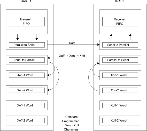 Figure 19. Software Flow Control Example
8.3.1.6 Software Flow Control Example
Assumptions: UART1 is transmitting a large text file to UART2. Both UARTs are using software flow control with single character Xoff (0F) and Xon (0D) tokens. Both have Xoff threshold (TCR [3:0] = F) set to 60 and Xon threshold (TCR[7:4] = 8) set to 32. Both have the interrupt receive threshold (TLR[7:4] = D) set to 52.
UART1 begins transmission and sends 52 characters, at which point UART2 generates an interrupt to its processor to service the RCV FIFO, but assumes the interrupt latency is fairly long. UART1 continues sending characters until a total of 60 characters have been sent. At this time UART2 transmits a 0F to UART1, informing UART1 to halt transmission. UART1 likely sends the 61st character while UART2 is sending the Xoff character. Now, UART2 is serviced and the processor reads enough data out of the RCV FIFO that the level drops to 32. UART2 now sends a 0D to UART1, informing UART1 to resume transmission.
8.3.1.7 Reset
Table 2 summarizes the state of outputs after reset.
Table 2. Register Reset Functions(1)
| REGISTER | RESET CONTROL | RESET STATE |
|---|---|---|
| Interrupt enable register | RESET | All bits cleared |
| Interrupt identification register | RESET | Bit 0 is set. All other bits cleared. |
| FIFO control register | RESET | All bits cleared |
| Line control register | RESET | Reset to 00011101 (1D hex) |
| Modem control register | RESET | All bits cleared |
| Line status register | RESET | Bits 5 and 6 set. All other bits cleared. |
| Modem status register | RESET | Bits 0 to 3 cleared. Bits 4 to 7 input signals. |
| Enhanced feature register | RESET | All bits cleared |
| Receiver holding register | RESET | Pointer logic cleared |
| Transmitter holding register | RESET | Pointer logic cleared |
| Transmission control register | RESET | All bits cleared |
| Trigger level register | RESET | All bits cleared |
| Alternate function register | RESET | All bits (except AFR4) cleared; AFR4 set |
Table 3 summarizes the state of outputs after reset.
Table 3. Signal Reset Functions
| SIGNAL | RESET CONTROL | RESET STATE |
|---|---|---|
| TX | RESET | High |
| RTS | RESET | High |
| DTR | RESET | High |
| RXRDYA–B | RESET | High |
| TXRDYA–B | RESET | Low |
8.3.1.8 Interrupts
The TL16C752D UART has interrupt generation and prioritization (six prioritized levels of interrupts) capability. The interrupt enable register (IER) enables each of the six types of interrupts and the INT signal in response to an interrupt generation. The IER also can disable the interrupt system by clearing bits 0 to 3, 5 to 7. When an interrupt is generated, the interrupt identification register (IIR) indicates that an interrupt is pending and provides the type of interrupt through IIR[5−0]. Table 4 summarizes the interrupt control functions.
Table 4. Interrupt Control Functions
| IIR[5–0] | PRIORITY LEVEL | INTERRUPT TYPE | INTERRUPT SOURCE | INTERRUPT RESET METHOD |
|---|---|---|---|---|
| 000001 | None | None | None | None |
| 000110 | 1 | Receiver line status | OE, FE, PE, or BI errors occur in characters in the RX FIFO | FE < PE < BI: All erroneous characters are read from the RX FIFO. OE: Read LSR |
| 001100 | 2 | RX timeout | Stale data in RX FIFO | Read RHR |
| 000100 | 2 | RHR interrupt | DRDY (data ready) (FIFO disable) RX FIFO above trigger level (FIFO enable) |
Read RHR |
| 000010 | 3 | THR interrupt | TFE (THR empty) (FIFO disable) TX FIFO passes above trigger level (FIFO enable) |
Read IIR or a write to the THR |
| 000000 | 4 | Modem status | MSR[3:0] = 0 | Read MSR |
| 010000 | 5 | Xoff interrupt | Receive Xoff character or characters/special character | Receive Xon character or characters/Read of IIR |
| 100000 | 6 | CTS, RTS | RTS pin or CTS pin change state from active (low) to inactive (high) | Read IIR |
It is important to note that for the framing error, parity error, and break conditions, LSR[7] generates the interrupt. LSR[7] is set when there is an error anywhere in the RX FIFO and is cleared only when there are no more errors remaining in the FIFO. LSR[4–2] always represent the error status for the received character at the top of the RX FIFO. Reading the RX FIFO updates LSR[4–2] to the appropriate status for the new character at the top of the FIFO. If the RX FIFO is empty, then LSR[4–2] is all 0.
For the Xoff interrupt, if an Xoff flow character detection caused the interrupt, the interrupt is cleared by an Xon flow character detection. If a special character detection caused the interrupt, the interrupt is cleared by a read of the ISR.
8.3.1.9 Interrupt Mode Operation
In interrupt mode (if any bit of IER[3:0] is 1), the processor is informed of the status of the receiver and transmitter by an interrupt signal, INT. Therefore, it is not necessary to continuously poll the line status register (LSR) to see if any interrupt needs to be serviced. Figure 20 shows interrupt mode operation.
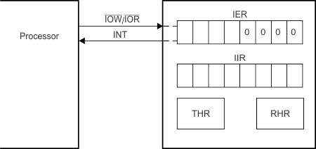 Figure 20. Interrupt Mode Operation
8.3.1.10 Polled Mode Operation
In polled mode (IER[3:0] = 0000), the status of the receiver and transmitter can then be checked by polling the line status register (LSR). This mode is an alternative to the interrupt mode of operation where the status of the receiver and transmitter is automatically known by means of interrupts sent to the CPU. Figure 21 shows polled mode operation.
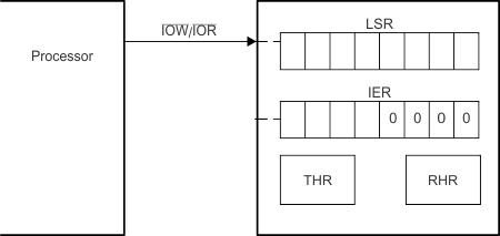 Figure 21. FIFO Polled Mode Operation
8.3.1.11 Break and Timeout Conditions
An RX timeout condition is detected when the receiver line, RX, has been high for a time equivalent to (4 × programmed word length) + 12 bits and there is at least one byte stored in the RX FIFO.
When a break condition occurs, the TX line is pulled low. A break condition is activated by setting LCR[6].
8.3.1.12 Programmable Baud Rate Generator
The TL16C752D UART contains a programmable baud generator that divides reference clock by a divisor in the range between 1 and (216 − 1). The output frequency of the baud rate generator is 16× the baud rate. An additional divide-by-4 prescaler is also available and can be selected by MCR[7], as shown in the following. The formula for the divisor is:
Where

Figure 22 shows the internal prescaler and baud rate generator circuitry.
 Figure 22. Prescaler and Baud Rate Generator Block Diagram
DLL and DLH must be written to in order to program the baud rate. DLL and DLH are the least significant and most significant byte of the baud rate divisor. If DLL and DLH are both 0, the UART is effectively disabled, because no baud clock is generated. The programmable baud rate generator is provided to select both the transmit and receive clock rates. Table 5 and Table 6 show the baud rate and divisor correlation for the crystal with frequency 1.8432 and 3.072 MHz, respectively.
Table 5. Baud Rates Using a 1.8432-MHz Crystal
| DESIRED BAUD RATE | DIVISOR USED TO GENERATE 16× CLOCK | PERCENT ERROR DIFFERENCE BETWEEN DESIRED AND ACTUAL |
|---|---|---|
| 50 | 2304 | |
| 75 | 1536 | |
| 110 | 1047 | 0.026 |
| 134.5 | 857 | 0.058 |
| 150 | 768 | |
| 300 | 384 | |
| 600 | 192 | |
| 1200 | 96 | |
| 1800 | 64 | |
| 2000 | 58 | 0.69 |
| 2400 | 48 | |
| 3600 | 32 | |
| 4800 | 24 | |
| 7200 | 16 | |
| 9600 | 12 | |
| 19200 | 6 | |
| 38400 | 3 | |
| 56000 | 2 | 2.86 |
Table 6. Baud Rates Using a 3.072-MHz Crystal
| DESIRED BAUD RATE | DIVISOR USED TO GENERATE 16× CLOCK | PERCENT ERROR DIFFERENCE BETWEEN DESIRED AND ACTUAL |
|---|---|---|
| 50 | 3840 | |
| 75 | 2560 | |
| 110 | 1745 | 0.026 |
| 134.5 | 1428 | 0.034 |
| 150 | 1280 | |
| 300 | 640 | |
| 600 | 320 | |
| 1200 | 160 | |
| 1800 | 107 | 0.312 |
| 2000 | 96 | |
| 2400 | 80 | |
| 3600 | 53 | 0.628 |
| 4800 | 40 | |
| 7200 | 27 | 1.23 |
| 9600 | 20 | |
| 19200 | 10 | |
| 38400 | 5 |
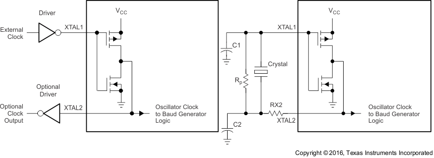
Figure 23 shows the crystal clock circuit reference.
8.4 Device Functional Modes
8.4.1 DMA Signaling
There are two modes of DMA operation, DMA mode 0 or 1, selected by FCR[3].
In DMA mode 0 or FIFO disable (FCR[0] = 0), DMA occurs in single character transfers. In DMA mode 1, multicharacter (or block) DMA transfers are managed to relieve the processor for longer periods of time.
8.4.1.1 Single DMA Transfers (DMA Mode0 or FIFO Disable)
Transmitter: When empty, the TXRDY signal becomes active. TXRDY goes inactive after one character has been loaded into it.
Receiver: RXRDY is active when there is at least one character in the FIFO. It becomes inactive when the receiver is empty.
Figure 24 shows TXRDY and RXRDY in DMA mode 0 or FIFO disable.
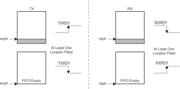 Figure 24. TXRDY and RXRDY in DMA Mode 0 or FIFO Disable
8.4.1.2 Block DMA Transfers (DMA Mode 1)
Transmitter: TXRDY is active when a trigger level number of spaces are available. It becomes inactive when the FIFO is full.
Receiver: RXRDY becomes active when the trigger level has been reached or when a timeout interrupt occurs. It goes inactive when the FIFO is empty or an error in the RX FIFO is flagged by LSR(7).
Figure 25 shows TXRDY and RXRDY in DMA mode 1.
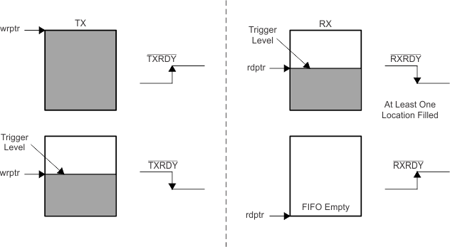 Figure 25. TXRDY and RXRDY in DMA Mode 1
8.4.2 Sleep Mode
Sleep mode is an enhanced feature of the TL16C752D UART. It is enabled when EFR[4], the enhanced functions bit, is set and when IER[4] is set. Sleep mode is entered when:
- The serial data input line, RX, is idle (see Break and Timeout Conditions).
- The TX FIFO and TX shift register are empty.
- There are no interrupts pending except THR and timeout interrupts.
Sleep mode is not entered if there is data in the RX FIFO.
In sleep mode, the UART clock and baud rate clock are stopped. Because most registers are clocked using these clocks, the power consumption is greatly reduced. The UART wakes up when any change is detected on the RX line, when there is any change in the state of the modem input pins, or if data is written to the TX FIFO.
NOTE
Writing to the divisor latches, DLL and DLH, to set the baud clock, must not be done during sleep mode. Therefore, TI recommends to disable sleep mode using IER[4] before writing to DLL or DLH.
8.5 Register Maps
8.5.1 Principals of Operation
Each register is selected using address lines A[0], A[1], A[2], and in some cases, bits from other registers. The programming combinations for register selection are shown in Figure 26.
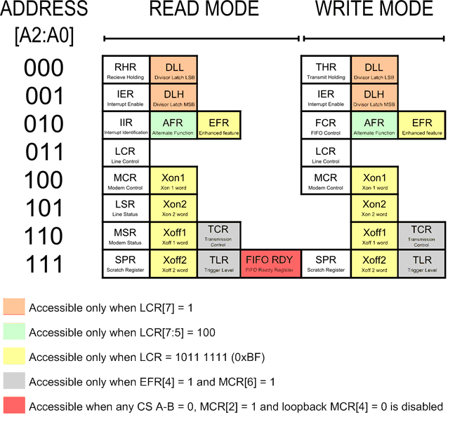
NOTE:
MCR[7:5], FCR[5:4], and IER[7:4] can only be modified when EFR[4] is set.Table 7 lists and describes the TL16C752D internal registers.
Table 7. TL16C752D Internal Registers(1) (2)
| ADDRESS | REGISTER | R/W (3) |
ACCESS CONSIDERATION | BIT 7 | BIT 6 | BIT 5 | BIT 4 | BIT 3 | BIT 2 | BIT 1 | BIT 0 |
|---|---|---|---|---|---|---|---|---|---|---|---|
| 0 0 0 | RHR | R | LCR[7] = 0 | bit 7 0 |
bit 6 0 |
bit 5 0 |
bit 4 0 |
bit 3 0 |
bit 2 0 |
bit 1 0 |
bit 0 0 |
| THR | W | bit 7 0 |
bit 6 0 |
bit 5 0 |
bit 4 0 |
bit 3 0 |
bit 2 0 |
bit 1 0 |
bit 0 0 |
||
| DLL(4) | RW | LCR[7] = 1 | bit 7 | bit 6 | bit 5 | bit 4 | bit 3 | bit 2 | bit 1 | bit 0 | |
| 0 0 1 | IER | RW | LCR[7] = 0 | CTS# Interrupt enable(1)
0 |
RTS# Interrupt enable(1)
0 |
Xoff Interrupt enable(1)
0 |
Sleep mode(1)
0 |
Modem status interrupt 0 |
RX line status interrupt 0 |
THR empty interrupt 0 |
RX data available interrupt 0 |
| DLH(4) | RW | LCR[7] = 1 | bit 7 | bit 6 | bit 5 | bit 4 | bit 3 | bit 2 | bit 1 | bit 0 | |
| 0 1 0 | IIR | R | LCR[7] = 0 | FCR(0) 0 |
FCR(0) 0 |
CTS# / RTS# 0 |
Xoff 0 |
Interrupt priority bit 2 0 |
Interrupt priority bit 1 0 |
Interrupt priority bit 0 0 |
Interrupt status 1 |
| FCR | W | RX trigger level 0 |
RX trigger level 0 |
TX trigger level(1)
0 |
TX trigger level(1)
0 |
DMA mode select 0 |
Resets TX FIFO 0 |
Resets RX FIFO 0 |
Enable FIFOs 0 |
||
| AFR(5) | RW | LCR[7:5] = 100 | DLY2 0 |
DLY1 0 |
DLY0 0 |
RCVEN 1 |
485LG 0 |
485RN 0 |
IREN 0 |
CONC 0 |
|
| EFR(6) | RW | LCR[7:0] = 10111111 | Auto CTS# 0 |
Auto RTS# 0 |
Special character detect 0 |
Enable enhanced functions 0 |
S/W flow control bit 3 0 |
S/W flow control bit 2 0 |
S/W flow control bit 1 0 |
S/W flow control bit 0 0 |
|
| 0 1 1 | LCR | RW | None | DLAB & EFR enable 0 |
Break control bit 0 |
Sets parity 0 |
Parity type select 1 |
Parity enable 1 |
No. of stop bits 1 |
Word length 0 |
Word length 1 |
| 1 0 0 | MCR | RW | LCR[7:0] ≠ 10111111 | 1x / 4x clock(1)
0 |
TCR & TLR enable(1)
0 |
Xon any(1)
0 |
Enable loopback 0 |
IRQ enable 0 |
FIFORdy enable 0 |
RTS# 0 |
DTR# 0 |
| Xon1(6) | RW | LCR[7:0] = 10111111 | bit 7 1 |
bit 6 1 |
bit 5 1 |
bit 4 1 |
bit 3 1 |
bit 2 1 |
bit 1 1 |
bit 0 1 |
|
| 1 0 1 | LSR | R | LCR[7:0] ≠ 10111111 | Error in RX FIFO 0 |
THR & TSR empty 1 |
THR empty 1 |
Break interrupt 0 |
Framing error 0 |
Parity error 0 |
Overrun error 0 |
Data in receiver 0 |
| Xon2(6) | RW | LCR[7:0] = 10111111 | bit 7 1 |
bit 6 1 |
bit 5 1 |
bit 4 0 |
bit 3 1 |
bit 2 1 |
bit 1 1 |
bit 0 1 |
|
| 1 1 0 | MSR | R | LCR[7:0] ≠ 10111111 | CD# 1 |
RI# 1 |
DSR# 1 |
CTS# 0 |
∆CD# 0 |
∆RI# 0 |
∆DSR# 0 |
∆CTS# 0 |
| Xoff1(6) | RW | LCR[7:0] = 10111111 | bit 7 1 |
bit 6 1 |
bit 5 1 |
bit 4 1 |
bit 3 1 |
bit 2 1 |
bit 1 1 |
bit 0 1 |
|
| TCR(7) | RW | EFR[4] = 1 & MCR[6] = 1 | bit 7 0 |
bit 6 0 |
bit 5 0 |
bit 4 0 |
bit 3 0 |
bit 2 0 |
bit 1 0 |
bit 0 0 |
|
| 1 1 1 | SPR | RW | LCR[7:0] ≠ 10111111 | bit 7 1 |
bit 6 1 |
bit 5 1 |
bit 4 1 |
bit 3 1 |
bit 2 1 |
bit 1 1 |
bit 0 1 |
| Xoff2(6) | RW | LCR[7:0] = 10111111 | bit 7 1 |
bit 6 1 |
bit 5 1 |
bit 4 1 |
bit 3 1 |
bit 2 1 |
bit 1 1 |
bit 0 1 |
|
| TLR(7) | RW | EFR[4] = 1 & MCR[6] = 1 | bit 7 0 |
bit 6 0 |
bit 5 0 |
bit 4 0 |
bit 3 0 |
bit 2 0 |
bit 1 0 |
bit 0 0 |
|
| FIFORdy(8) | R | MCR[4] = 0 & MCR[2] = 1 | RX FIFO D status 0 |
RX FIFO C status 0 |
RX FIFO B status 0 |
RX FIFO A status 0 |
TX FIFO D status 0 |
TX FIFO C status 0 |
TX FIFO B status 0 |
TX FIFO A status 0 |
8.5.2 Receiver Holding Register (RHR)
The receiver section consists of the RHR and the receiver shift register (RSR). The RHR is actually a 64-byte FIFO. The RSR receives serial data from RX terminal. The data is converted to parallel data and moved to the RHR. The receiver section is controlled by the line control register. If the FIFO is disabled, location 0 of the FIFO is used to store the characters. If overflow occurs, characters are lost. The RHR also stores the error status bits associated with each character.
8.5.3 Transmit Holding Register (THR)
The transmitter section consists of the THR and the transmitter shift register (TSR). The transmit holding register is actually a 64-byte FIFO. The THR receives data and shifts it into the TSR where it is converted to serial data and moved out on the TX terminal. If the FIFO is disabled, location 0 of the FIFO is used to store the byte. Characters are lost if overflow occurs.
8.5.4 FIFO Control Register (FCR)
This is a write-only register which is used for enabling the FIFOs, clearing the FIFOs, setting transmitter and receiver trigger levels, and selecting the type of DMA signaling. Table 8 shows FIFO control register bit settings.
Table 8. FCR Bit Settings
| BIT | BIT SETTINGS |
|---|---|
| 0 | 0 = Disable the transmit and receive FIFOs 1 = Enable the transmit and receive FIFOs |
| 1 | 0 = No change 1 = Clears the receive FIFO and resets its counter logic to 0. Returns to 0 after clearing FIFO. |
| 2 | 0 = No change 1 = Clears the transmit FIFO and resets its counter logic to 0. Returns to 0 after clearing FIFO. |
| 3 | 0 = DMA mode 0 1 = DMA mode 1 |
| 5:4(1) | Sets the trigger level for the TX FIFO: 00 – 8 spaces 01 – 16 spaces 10 – 32 spaces 11 – 56 spaces |
| 7:6 | Sets the trigger level for the RX FIFO: 00 – 1 characters 01 – 4 characters 10 – 56 characters 11 – 60 characters |
8.5.5 Line Control Register (LCR)
This register controls the data communication format. The word length, number of stop bits, and parity type are selected by writing the appropriate bits to the LCR. Table 9 shows line control register bit settings.
Table 9. LCR Bit Settings
| BIT | BIT SETTINGS |
|---|---|
| 1:0 | Specifies the word length to be transmitted or received 00 – 5 bits 01 – 6 bits 10 − 7 bits 11 – 8 bits |
| 2 | Specifies the number of stop bits: 0 – 1 stop bits (Word length = 5, 6, 7, 8) 1 – 1.5 stop bits (Word length = 5) 1 – 2 stop bits (Word length = 6, 7, 8) 3 |
| 3 | 0 = No parity 1 = A parity bit is generated during transmission and the receiver checks for received parity. |
| 4 | 0 = Odd parity is generated (if LCR[3] = 1) 1 = Even parity is generated (if LCR[3] = 1) |
| 5 | Selects the forced parity format (if LCR(3) = 1) If LCR[5] = 1 and LCR[4] = 0 the parity bit is forced to 1 in the transmitted and received data. If LCR[5] = 1 and LCR[4] = 1 the parity bit is forced to 0 in the transmitted and received data. |
| 6 | Break control bit 0 = Normal operating condition 1 = Forces the transmitter output to go low to alert the communication terminal. |
| 7 | 0 = Normal operating condition 1 = Divisor latch enable |
8.5.6 Line Status Register (LSR)
Table 10 shows line status register bit settings.
Table 10. LSR Bit Settings
| BIT | BIT SETTINGS |
|---|---|
| 0 | 0 = No data in the receive FIFO 1 = At least one character in the RX FIFO |
| 1 | 0 = No overrun error 1 = Overrun error has occurred. |
| 2 | 0 = No parity error in data being read from RX FIFO 1 = Parity error in data being read from RX FIFO |
| 3 | 0 = No framing error in data being read from RX FIFO 1 = Framing error occurred in data being read from RX FIFO (that is, received data did not have a valid stop bit) |
| 4 | 0 = No break condition 1 = A break condition occurred and associated byte is 00 (that is, RX was low for at least one character time frame) |
| 5 | 0 = Transmit hold register is not empty 1 = Transmit hold register is empty. The processor can now load up to 64 bytes of data into the THR if the TX FIFO is enabled. |
| 6 | 0 = Transmitter hold and shift registers are not empty. 1 = Transmitter hold and shift registers are empty. |
| 7 | 0 = Normal operation 1 = At least one parity error, framing error or break indication are stored in the receiver FIFO. Bit 7 is cleared when no errors are present in the FIFO. |
When the LSR is read, LSR[4:2] reflects the error bits [BI, FE, PE] of the character at the top of the RX FIFO (next character to be read). The LSR[4:2] registers do not physically exist, as the data read from the RX FIFO is output directly onto the output data-bus, DI[4:2], when the LSR is read. Therefore, errors in a character are identified by reading the LSR and then reading the RHR.
LSR[7] is set when there is an error anywhere in the RX FIFO and is cleared only when there are no more errors remaining in the FIFO.
NOTE
Reading the LSR does not cause an increment of the RX FIFO read pointer. The RX FIFO read pointer is incremented by reading the RHR.
8.5.7 Modem Control Register (MCR)
The MCR controls the interface with the modem, data set, or peripheral device that is emulating the modem. Table 11 shows modem control register bit settings.
Table 11. MCR Bit Settings(1)
| BIT | BIT SETTINGS |
|---|---|
| 0 | 0 = Force DTR output to inactive (high) 1 = Force DTR output to active (low). In loopback controls MSR[5] |
| 1 | 0 = Force RTS output to inactive (high) 1 = Force RTS output to active (low) In loopback controls MSR[4] If Auto-RTS is enabled the RTS output is controlled by hardware flow control |
| 2 | 0 Disables the FIFORdy register 1 Enable the FIFORdy register In loopback controls MSR[6] |
| 3 | 0 = Forces the IRQ(A-B) outputs to high-impedance state 1 = Forces the IRQ(A-B) outputs to the active state In loopback controls MSR[7] |
| 4 | 0 = Normal operating mode 1 = Enable local loopback mode (internal) In this mode, the MCR[3:0] signals are looped back into MSR[3:0] and the TX output is looped back to the RX input internally |
| 5 | 0 = Disable Xon Any function 1 = Enable Xon Any function |
| 6 | 0 = No action 1 = Enable access to the TCR and TLR registers |
| 7 | 0 = Divide by one clock input 1 = Divide by four clock input This bit reflects the inverse of the CLKSEL pin value at the trailing edge of the RESET pulse |
8.5.8 Modem Status Register (MSR)
This 8-bit register provides information about the current state of the control lines from the modem, data set, or peripheral device to the processor. It also indicates when a control input from the modem changes state. Table 12 shows modem status register bit settings.
Table 12. MSR Bit Settings(1)
| BIT | BIT SETTINGS |
|---|---|
| 0 | Indicates that CTS input (or MCR[1] in loopback) has changed state. Cleared on a read. |
| 1 | Indicates that DSR input (or MCR[0] in loopback) has changed state. Cleared on a read. |
| 2 | Indicates that RI input (or MCR[2] in loopback) has changed state from low to high. Cleared on a read. |
| 3 | Indicates that CD input (or MCR[3] in loopback) has changed state. Cleared on a read. |
| 4 | This bit is equivalent to MCR[1] during local loop-back mode. It is the complement to the CTS input. |
| 5 | This bit is equivalent to MCR[0] during local loop-back mode. It is the complement to the DSR input. |
| 6 | This bit is equivalent to MCR[2] during local loop-back mode. It is the complement to the RI input. |
| 7 | This bit is equivalent to MCR[3] during local loop-back mode. It is the complement to the CD input. |
8.5.9 Interrupt Enable Register (IER)
The interrupt enable register (IER) enables each of the six types of interrupt, receiver error, RHR interrupt, THR interrupt, Xoff received, or CTS/RTS change of state from low to high. The INT output signal is activated in response to interrupt generation. Table 13 shows interrupt enable register bit settings.
Table 13. Interrupt Enable Register (IER) Bit Settings(1)
| BIT | BIT SETTINGS |
|---|---|
| 0 | 0 = Disable the RHR interrupt 1 = Enable the RHR interrupt |
| 1 | 0 = Disable the THR interrupt 1 = Enable the THR interrupt |
| 2 | 0 = Disable the receiver line status interrupt 1 = Enable the receiver line status interrupt |
| 3 | 0 = Disable the modem status register interrupt 1 = Enable the modem status register interrupt |
| 4 | 0 = Disable sleep mode 1 = Enable sleep mode |
| 5 | 0 = Disable the Xoff interrupt 1 = Enable the Xoff interrupt |
| 6 | 0 = Disable the RTS interrupt 1 = Enable the RTS interrupt |
| 7 | 0 = Disable the CTS interrupt 1 = Enable the CTS interrupt |
Re-enabling IER[1] causes a new interrupt, if the THR is below the threshold.
8.5.10 Interrupt Identification Register (IIR)
The IIR is a read-only 8-bit register, which provides the source of the interrupt in a prioritized manner. Table 14 shows interrupt identification register bit settings.
Table 14. IIR Bit Settings
| BIT | BIT SETTINGS |
|---|---|
| 0 | 0 = An interrupt is pending 1 = No interrupt is pending |
| 3:1 | 3-Bit encoded interrupt. See Table 13 |
| 4 | 1 = Xoff or special character has been detected |
| 5 | CTS/RTS low to high change of state |
| 7:6 | Mirror the contents of FCR[0] |
The interrupt priority list is illustrated in Table 15.
Table 15. Interrupt Priority List
| PRIORITY LEVEL | BIT 5 | BIT 4 | BIT 3 | BIT 2 | BIT 1 | BIT 0 | INTERRUPT SOURCE |
|---|---|---|---|---|---|---|---|
| 1 | 0 | 0 | 0 | 1 | 1 | 0 | Receiver line status error |
| 2 | 0 | 0 | 1 | 1 | 0 | 0 | Receiver timeout interrupt |
| 2 | 0 | 0 | 0 | 1 | 0 | 0 | RHR interrupt |
| 3 | 0 | 0 | 0 | 0 | 1 | 0 | THR interrupt |
| 4 | 0 | 0 | 1 | 0 | 0 | 0 | Modem interrupt |
| 5 | 0 | 1 | 0 | 0 | 0 | 0 | Received Xoff signal or special character |
| 6 | 1 | 0 | 0 | 0 | 0 | 0 | CTS, RTS change of state from active (low) to inactive (high) |
8.5.11 Enhanced Feature Register (EFR)
This 8-bit register enables or disables the enhanced features of the UART. Table 16 shows the enhanced feature register bit settings.
Table 16. EFR Bit Settings
| BIT | BIT SETTINGS |
|---|---|
| 3:0 | Combinations of software flow control can be selected by programming bit 3 to bit 0. See Table 1. |
| 4 | Enhanced functions enable bit. 0 = Disables enhanced functions and writing to IER[7:4], FCR[5:4], MCR[7:5] 1 = Enables the enhanced function IER[7:4], FCR[5:4], and MCR[7:5] can be modified, that is, this bit is therefore a write enable |
| 5 | 0 = Normal operation 1 = Special character detect. Received data is compared with Xoff-2 data. If a match occurs, the received data is transferred to FIFO and IIR[4] is set to 1 to indicate a special character has been detected. |
| 6 | RTS flow control enable bit 0 = Normal operation 1 = RTS flow control is enabled, that is, RTS pin goes high when the receiver FIFO HALT trigger level TCR[3:0] is reached, and goes low when the receiver FIFO RESTORE transmission trigger level TCR[7:4] is reached. |
| 7 | CTS flow control enable bit 0 = Normal operation 1 = CTS flow control is enabled, that is, transmission is halted when a high signal is detected on the CTS pin |
8.5.12 Divisor Latches (DLL, DLH)
Two 8-bit registers store the 16-bit divisor for generation of the baud clock in the baud rate generator. DLH, stores the most significant part of the divisor. DLL stores the least significant part of the division.
DLL and DLH can only be written to before sleep mode is enabled (that is, before IER[4] is set).
8.5.13 Transmission Control Register (TCR)
This 8-bit register is used to store the receive FIFO threshold levels to start or stop transmission during hardware or software flow control. Table 17 shows transmission control register bit settings.
Table 17. TCR Bit Settings
| BIT | BIT SETTINGS |
|---|---|
| 3:0 | RCV FIFO trigger level to HALT transmission (0 to 60) |
| 7:4 | RCV FIFO trigger level to RESTORE transmission (0 to 60) |
TCR trigger levels are available from 0 to 60 bytes with a granularity of four.
TCR can be written to only when EFR[4] = 1 and MCR[6] = 1. The programmer must program the TCR such that TCR[3:0] > TCR[7:4]. There is no built-in hardware check to make sure this condition is met. Also, the TCR must be programmed with this condition before Auto-RTS or software flow control is enabled to avoid spurious operation of the device.
8.5.14 Trigger Level Register (TLR)
This 8-bit register is used to store the transmit and received FIFO trigger levels used for DMA and interrupt generation. Trigger levels from 4 to 60 can be programmed with a granularity of 4. Table 18 shows trigger level register bit settings.
Table 18. TLR Bit Settings
| BIT | BIT SETTINGS |
|---|---|
| 3:0 | Transmit FIFO trigger levels (4 to 60), number of spaces available |
| 7:4 | RCV FIFO trigger levels (4 to 60), number of characters available |
TLR can be written to only when EFR[4] = 1 and MCR[6] = 1. If TLR[3:0] or TLR[7:4] are 0, then the selectable trigger levels via the FIFO control register (FCR) are used for the transmit and receive FIFO trigger levels. Trigger levels from 4 to 60 bytes are available with a granularity of 4. The TLR should be programmed for N / 4, where N is the desired trigger level.
8.5.15 FIFO Ready Register
The FIFO ready register provides realtime status of the transmit and receive FIFOs of both channels. Table 19 shows the FIFO ready register bit settings. The trigger level mentioned in Table 19 refers to the setting in either FCR (when TLR value is 0), or TLR (when it has a nonzero value).
Table 19. FIFO Ready Register
| BIT | BIT SETTINGS |
|---|---|
| 0 | 0 = There are fewer than a TX trigger level number of spaces available in the TX FIFO of channel A. 1 = There are at least a TX trigger level number of spaces available in the TX FIFO of channel A. |
| 1 | 0 = There are fewer than a TX trigger level number of spaces available in the TX FIFO of channel B. 1 = There are at least a TX trigger level number of spaces available in the TX FIFO of channel B. |
| 3:2 | Unused, always 0 |
| 4 | 0 = There are fewer than a RX trigger level number of characters in the RX FIFO of channel A. 1 = The RX FIFO of channel A has more than a RX trigger level number of characters available for reading or a timeout condition has occurred. |
| 5 | 0 = There are fewer than a RX trigger level number of characters in the RX FIFO of channel B. 1 = The RX FIFO of channel B has more than a RX trigger level number of characters available for reading or a timeout condition has occurred. |
| 7:6 | Unused, always 0 |
The FIFORdy register is a read only register and can be accessed when any of the two UARTs are selected. CSA or CSB = 0, MCR[2] (FIFORdy Enable) is a logic 1, and loopback is disabled. Its address is 111.
8.5.16 Alternate Function Register (AFR)
The AFR is used to enable some extra functionality beyond the capabilities of the original TL16C752B. The first of these is a concurrent write mode, which can be useful in more expediently setting up all four UART channels. The second addition is the IrDA mode, which supports Standard IrDA (SIR) mode with baud rates from 2400 to 115.2 bps. The third addition is support for RS-485 bus drivers or transceivers by providing an output pin (DTRx) per channel, which is timed to keep the RS-485 driver enabled as long as transmit data is pending.
The AFR is located at A[2:0] = 010 when LCR[7:5] = 100.
Table 20. AFR Bit Settings
| BIT | BIT SETTINGS |
|---|---|
| 0 | CONC enables the concurrent write of all four (754) or two (752) channels simultaneously, which helps speed up initialization. Ensure that any indirect addressing modes have been enabled before using. |
| 1 | IREN enables the IrDA SIR mode. This mode is only specified to 115.2 bps; TI does not recommend the use of this mode at higher speeds. |
| 2 | 485EN enables the half duplex RS-485 mode and causes the DTRx output to be set high whenever there is any data in the THR or TSR and to be held high until the delay set by DLY2:0 has expired, at which time it is set low. The DTRx output is intended to drive the enabled input of an RS-485 driver. When this bit is set, the transmitter interrupts are held off until the TSR is empty, unless 485LG is set. |
| 3 | 485LG is set when the 485EN is set. This bit indicates that a relatively large data block is being set, requiring more than a single load of the xmt fifo. In this case, the transmitter interrupts occur as in the standard RS-232 mode, either when the xmt fifo contents drop below the xmt threshold or when the xmt fifo is empty. |
| 4 | RCVEN is valid only when 485EN or IREN is set, and allows the serial receiver to listen in or snoop on the RS485 traffic or IrDA traffic. RS485 mode is generally considered half duplex, and usually a node is either driving or receiving, but there can be cases when it is advantageous to verify what you are sending. This can be used to detect collisions or as part of an arbitration mechanism on the bus. When both RCVEN and 485EN are set, the receiver stores any data presented on RX, if any. Note that implies that the external RS485 receiver is enabled. Whenever 485EN is cleared, the serial receiver is enabled for normal full duplex RS232 traffic. If RCVEN is cleared while 485EN is set, the receiver is disabled while that channel is transmitting. SIR is also considered half duplex. Often the light energy from the transmitting LED is coupled back into the receiving PIN diode, which creates an input data stream that is not of interest to the host. Disabling the receiver (clearing RCVEN) prevents this reception, and eliminates the task of unloading the data. On the other hand, for diagnostic or other purposes, it may be useful to observe this data stream. For example, a mirror could be used to intentionally couple the output LED to the input PIN. For these cases, RCVEN could be set to enable the receiver. NOTE: When RCVEN is cleared (set to 0), the character timeout interrupt is not available, even in RSA-232 mode. This can be useful when checking code for valid threshold interrupts, as the timeout interrupt will not override the threshold interrupt. |
| 7:5 | DLY2 to DLY0 sets a delay after the last stop bit of the last data byte being set before the DTRx is set low, to allow for long cable runs. The delay is in number of bit times and is enabled by 485EN. The delay starts only when both the xmt serial shift register (TSR) is empty and the xmt fifo (THR) is empty, and if started, will be cleared by any data being written to the THR. |
Table 21. LOOP and RCVEN Functionality
| LOOP MODE | RCVEN | AFR | MODE | DESCRIPTION |
|---|---|---|---|---|
| LOOP mode off, MCR4 = 0, RX, TX active |
RCVEN = 1 | AFR = 10 | RS-232 | Receive threshold, timeout, and error detection interrupts available Data stored in receive FIFO |
| AFR = 14 | RS-485 | Receive threshold, timeout, and error detection interrupts available Data stored in receive FIFO |
||
| AFR = 12 | IrDA | Receive threshold, timeout, and error detection interrupts available Data stored in receive FIFO |
||
| RCVEN = 0 | AFR = 00 | RS-232 | Receive threshold and error detection interrupts available Data stored in receive FIFO |
|
| AFR = 04 | RS-485 | No data stored in receive FIFO, hence no interrupts available | ||
| AFR = 02 | IrDA | No data stored in receive FIFO, hence no interrupts available | ||
| LOOP mode on, MCR4 = 1, RX, TX inactive |
RCVEN = 1 | AFR = 10 | RS-232 | Receive threshold, timeout, and error detection interrupts available Data stored in receive FIFO |
| AFR = 14 | RS-485 | Receive threshold, timeout, and error detection interrupts available Data stored in receive FIFO |
||
| AFR = 12 | IrDA | Receive threshold, timeout, and error detection interrupts available Data stored in receive FIFO |
||
| RCVEN = 0 | AFR = 00 | RS-232 | Receive threshold and error detection interrupts available Data stored in receive FIFO |
|
| AFR = 04 | RS-485 | Receive threshold and error detection interrupts available Data stored in receive FIFO |
||
| AFR = 02 | IrDA | Receive threshold and error detection interrupts available Data stored in receive FIFO |
8.5.17 RS-485 Mode
The RS-485 mode is intended to simplify the interface between the UART channel and an RS-485 driver or transceiver. When enabled by setting 485EN, the DTRx output goes high one bit time before the first stop bit of the first data byte being sent, and remains high as long as there is pending data in the TSR or THR (xmt fifo). After both are empty (after the last stop bit of the last data byte), the DTRx output stays high for a programmable delay of 0 to 15 bit times, as set by DLY[2:0]. This helps preserve data integrity over long signal lines. This is illustrated in the following.
Often RS-485 packets are relatively short and the entire packet can fit within the 64 byte xmt fifo. In this case, it goes empty when the TSR goes empty. But in cases where a larger block needs to be sent, it is advantageous to reload the xmt fifo as soon as it is depleted. Otherwise, the transmission stalls while waiting for the xmt fifo to be reloaded, which varies with processor load. In this case, it is best to also set 485LG (large block), which causes the transmit interrupt to occur wither when the THR becomes empty (if the xmt fifo level was not above the threshold), or when the xmt fifo threshold is crossed. The reloading of the xmt fifo occurs while some data is being shifted out, eliminating fifo underrun. If desired, when the last bytes of a current transmission are being loaded in the xmt fifo, 485LG can be cleared before the load and the transmit interrupt occurs on the TSR going empty.

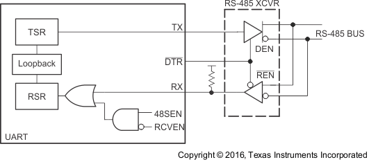 Figure 28. RS-485 Application Example 1
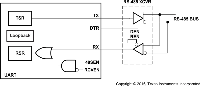 Figure 29. RS-485 Application Example 2
8.5.18 IrDA Overview
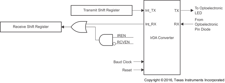 Figure 30. IrDA Mode
The IrDA defines several protocols for sending and receiving serial infrared data, including rates of 115.2 kbps, 0.576 Mbps, 1.152 Mbps, and 4 Mbps. The low rate of 115.2 kbps was specified first and the others must maintain downward compatibility with it. At the 115.2 kbps rate, the protocol implemented in the hardware is fairly simple. It primarily defines a serial infrared data word to be surrounded by a start bit equal to 0 and a stop bit equal to 1. Individual bits are encoded or decoded the same whether they are start, data, or stop bits. The IrDA engine in the TL16C752D device only evaluates single bits and follows the 115.2-kbps protocol. The 115.2-kbps rate is a maximum rate. When both ends of the transfer are setup to a lower but matching speed, the protocol still works. The clock used to code or sample the data is 16 times the baud rate, or 1.843-MHz maximum. To code a 1, no pulse is sent or received for 1-bit time period, or 16 clock cycles. To code a 0, one pulse is sent or received within a 1-bit time period, or 16 clock cycles. The pulse must be at least 1.6-μs wide and 3 clock cycles long at 1.843 MHz. At lower baud rates the pulse can be 1.6 μs wide or as long as 3 clock cycles. The transmitter output, TX, is intended to drive a LED circuit to generate an infrared pulse. The LED circuits work on positive pulses. A terminal circuit is expected to create the receiver input, RX. Most, but not all, PIN circuits have inversion and generate negative pulses from the detected infrared light. Their output is normally high. The TL16C752D device can decode either negative or positive pulses on RX.
8.5.19 IrDA Encoder Function
Serial data from a UART is encoded to transmit data to the optoelectronics. While the serial data input to this block (Int_TX) is high, the output (TX) is always low, and the counter used to form a pulse on TX is continuously cleared. After Int_TX resets to 0, TX rises on the falling edge of the 7th 16XCLK. On the falling edge of the 10th 16XCLK pulse, TX falls, creating a 3-clock-wide pulse. While Int_TX stays low, a pulse is transmitted during the seventh to tenth clocks of each 16-clock bit cycle.
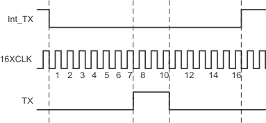 Figure 31. IrDA-SIR Encoding Scheme – Detailed Timing Diagram
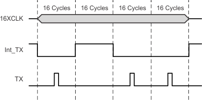 Figure 32. Encoding Scheme – Macro View
After reset, Int_RX is high and the 4-bit counter is cleared. When a falling edge is detected on RX, Int_RX falls on the next rising edge of 16XCLK with sufficient setup time. Int_RX stays low for 16 cycles (16XCLK) and then returns to high as required by the IrDA specification. As long as no pulses (falling edges) are detected on RX, Int_RX remains high.
 Figure 33. IrDA-SIR Decoding Scheme – Detailed Timing Diagram
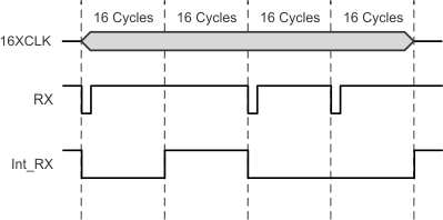 Figure 34. IrDA-SIR Decoding Scheme – Macro View
It is possible for jitter or slight frequency differences to cause the next falling edge on RX to be missed for one 16XCLK cycle. In that case, a 1-clock-wide pulse appears on Int_RX between consecutive 0s. It is important for the UART to strobe Int_RX in the middle of the bit time to avoid latching this 1-clock-wide pulse. The TL16C550C UART already strobes incoming serial data at the proper time. Otherwise, note that data is required to be framed by a leading 0 and a trailing 1. The falling edge of that first 0 on Int_RX synchronizes the read strobe. The strobe occurs on the 8th 16XCLK pulse after the Int_RX falling edge and once every 16 cycles thereafter until the stop bit occurs.
 Figure 35. Timing Causing 1-Clock-Wide Pulse Between Consecutive Ones
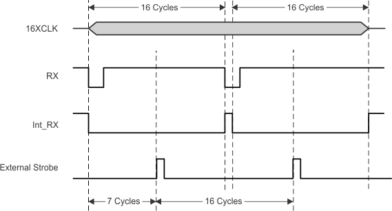 Figure 36. Recommended Strobing for Decoded Data
The TL16C752D device can decode positive pulses on RX. The timing is different, but the variation is invisible to the UART. The decoder, which works from the falling edge, now recognizes a 0 on the trailing edge of the pulse rather than on the leading edge. As long as the pulse duration is fairly constant, as defined by the specification, the trailing edges should also be 16 clock cycles apart and data can readily be decoded. The 0 appears on Int_RX after the pulse rather than at the start of it.
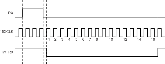 Figure 37. Positive RX Pulse Decode – Detailed View
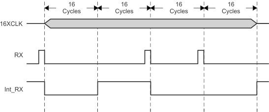 Figure 38. Positive RX Pulse Decode – Macro View