JAJSIJ1G October 2009 – August 2023 TL331-Q1 , TL331B-Q1 , TL391B-Q1
PRODMIX
- 1
- 1 特長
- 2 アプリケーション
- 3 概要
- 4 Revision History
- 5 Pin Configuration and Functions
-
6 Specifications
- 6.1 Absolute Maximum Ratings, TL331-Q1
- 6.2 Absolute Maximum Ratings, TL331B-Q1 and TL391B-Q1
- 6.3 ESD Ratings, All Devices
- 6.4 Recommended Operating Conditions, TL331-Q1
- 6.5 Recommended Operating Conditions, TL331B-Q1 and TL391B-Q1
- 6.6 Thermal Information
- 6.7 Electrical Characteristics, TL331B-Q1 and TL391B-Q1
- 6.8 Switching Characteristics, TL331B-Q1 and TL391B-Q1
- 6.9 Electrical Characteristics, TL331-Q1
- 6.10 Switching Characteristics, TL331-Q1
- 6.11 Typical Characteristics, TL331-Q1
- 6.12 Typical Characteristics, TL331B-Q1 and TL391B-Q1
- 7 Detailed Description
- 8 Application and Implementation
- 9 Device and Documentation Support
- 10Mechanical, Packaging, and Orderable Information
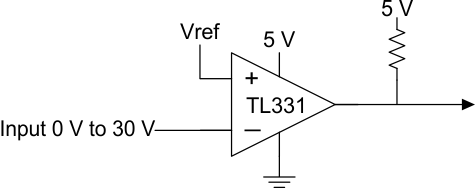
8.2 Typical Application
 Figure 8-1 Typical Application Schematic