JAJSIJ1G October 2009 – August 2023 TL331-Q1 , TL331B-Q1 , TL391B-Q1
PRODMIX
- 1
- 1 特長
- 2 アプリケーション
- 3 概要
- 4 Revision History
- 5 Pin Configuration and Functions
-
6 Specifications
- 6.1 Absolute Maximum Ratings, TL331-Q1
- 6.2 Absolute Maximum Ratings, TL331B-Q1 and TL391B-Q1
- 6.3 ESD Ratings, All Devices
- 6.4 Recommended Operating Conditions, TL331-Q1
- 6.5 Recommended Operating Conditions, TL331B-Q1 and TL391B-Q1
- 6.6 Thermal Information
- 6.7 Electrical Characteristics, TL331B-Q1 and TL391B-Q1
- 6.8 Switching Characteristics, TL331B-Q1 and TL391B-Q1
- 6.9 Electrical Characteristics, TL331-Q1
- 6.10 Switching Characteristics, TL331-Q1
- 6.11 Typical Characteristics, TL331-Q1
- 6.12 Typical Characteristics, TL331B-Q1 and TL391B-Q1
- 7 Detailed Description
- 8 Application and Implementation
- 9 Device and Documentation Support
- 10Mechanical, Packaging, and Orderable Information
5 Pin Configuration and Functions

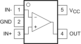
Note reversed
inputs compared to similar popular pinout
Figure 5-1 TL331-Q1, TL331B-Q1 DBV Package5-Pin SOT-23
Top View

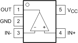
Note reversed
inputs compared to similar popular pinout
Figure 5-2 TL391B-Q1 DBV Package5-Pin SOT-23
Top View
Table 5-1 Pin Functions
| PIN | TYPE | DESCRIPTION | ||
|---|---|---|---|---|
| TL331-Q1, TL331B-Q1 | TL391B-Q1 | |||
| NAME | NO. | NO. | ||
| IN+ | 3 | 4 | I | Positive Input |
| IN– | 1 | 3 | I | Negative Input |
| OUT | 4 | 1 | O | Open Collector/Drain Output |
| VCC | 5 | 5 | — | Power Supply Input |
| GND | 2 | 2 | — | Ground |