SLVS641B April 2008 – March 2015 TL4242
PRODUCTION DATA.
- 1 Features
- 2 Applications
- 3 Description
- 4 Revision History
- 5 Pin Configuration and Functions
- 6 Specifications
- 7 Detailed Description
- 8 Application and Implementation
- 9 Power Supply Recommendations
- 10Layout
- 11Device and Documentation Support
- 12Mechanical, Packaging, and Orderable Information
パッケージ・オプション
メカニカル・データ(パッケージ|ピン)
- DRJ|8
サーマルパッド・メカニカル・データ
- DRJ|8
発注情報
6 Specifications
6.1 Absolute Maximum Ratings
over operating free-air temperature range (unless otherwise noted)(1)| MIN | MAX | UNIT | |||
|---|---|---|---|---|---|
| VCC | Supply voltage(2) | –42 | 45 | V | |
| VI | Input voltage | D | –0.3 | 7 | V |
| PWM | –40 | 40 | |||
| REF | –1 | 16 | |||
| VO | Output voltage | Q | –1 | 41 | V |
| ST | –0.3 | 40 | |||
| IO | Output current | PWM | ±1 | mA | |
| REF | ±2 | ||||
| ST | ±5 | ||||
| TJ | Virtual-junction temperature | –40 | 150 | °C | |
| Tstg | Storage temperature | –50 | 150 | °C | |
(1) Stresses beyond those listed under Absolute Maximum Ratings may cause permanent damage to the device. These are stress ratings only, and functional operation of the device at these or any other conditions beyond those indicated under Recommended Operating Conditions is not implied. Exposure to absolute-maximum-rated conditions for extended periods may affect device reliability.
(2) All voltage values are with respect to the network ground terminal.
6.2 ESD Ratings
| VALUE | UNIT | |||
|---|---|---|---|---|
| V(ESD) | Electrostatic discharge | Human-body model (HBM), per ANSI/ESDA/JEDEC JS-001(1) | ±1000 | V |
| Charged-device model (CDM), per JEDEC specification JESD22-C101(2) | ±1000 | |||
(1) JEDEC document JEP155 states that 500-V HBM allows safe manufacturing with a standard ESD control process.
(2) JEDEC document JEP157 states that 250-V CDM allows safe manufacturing with a standard ESD control process.
6.3 Recommended Operating Conditions
| MIN | MAX | UNIT | ||
|---|---|---|---|---|
| VCC | Supply voltage | 4.5 | 42 | V |
| VST | Status (ST) output voltage | 16 | V | |
| VPWM | PWM voltage | 0 | 40 | V |
| CD | Status delay (D) capacitance | 0 | 2.2 | μF |
| RREF | Reference (REF) resistor | 0 | 10 | Ω |
| TJ | Virtual-junction temperature | –40 | 150 | °C |
6.4 Thermal Information
| THERMAL METRIC(1) | TL4242 | UNIT | ||
|---|---|---|---|---|
| DRJ (WSON) | ||||
| 8 PINS | ||||
| RθJA | Junction-to-ambient thermal resistance | 39.0 | °C/W | |
| RθJC(top) | Junction-to-case (top) thermal resistance | 31.5 | ||
| RθJB | Junction-to-board thermal resistance | 15.5 | ||
| ψJT | Junction-to-top characterization parameter | 0.3 | ||
| ψJB | Junction-to-board characterization parameter | 15.6 | ||
| RθJC(bot) | Junction-to-case (bottom) thermal resistance | 1.8 | ||
(1) For more information about traditional and new thermal metrics, see the IC Package Thermal Metrics application report, SPRA953.
6.5 Electrical Characteristics
over recommended operating free-air temperature range, VI = 13.5 V, RREF = 0.47 Ω, VPWM,H, TJ = –40°C to 150°C, all voltages with respect to ground (unless otherwise noted)| PARAMETER | TEST CONDITIONS | MIN | TYP | MAX | UNIT | |
|---|---|---|---|---|---|---|
| IqL | Supply current | VQ = 6.6 V | 12 | 22 | mA | |
| IqOFF | Supply current, off mode | PWM = L, TJ < 85°C | 0.1 | 2 | μA | |
| OUTPUT ELECTRICAL CHARACTERISTICS | ||||||
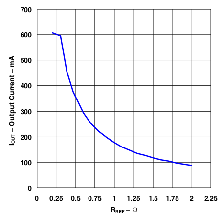
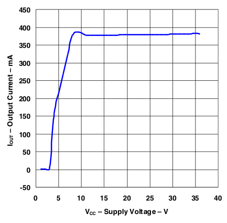
| IQ | Output current | VQ – VREF(1) = 6.6 V | 357 | 376 | 395 | mA |
| VQ – VREF = 6.6 V, RREF = 1 Ω | 168 | 177 | 185 | |||
| VQ – VREF = 6.6 V, RREF = 0.39 Ω | 431 | 454 | 476 | |||
| VQ – VREF = 5.4 V to 7.8 V, VI = 9 V to 16 V | 357 | 376 | 395 | |||
| IQmax | Output current limit | RREF = 0 Ω | 600 | mA | ||
| Vdr | Drop voltage | IQ = 300 mA | 0.35 | 0.7 | V | |
| PWM INPUT ELECTRICAL CHARACTERISTICS | ||||||
| VPWM,H | High-level PWM voltage | 2.6 | V | |||
| VPWM,L | Low-level PWM voltage | 0.7 | V | |||
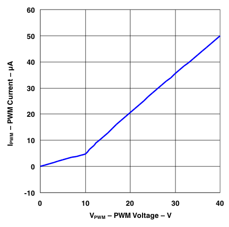
| IPWM,H | High-level PWM input current | VPWM = 5 V | 220 | 500 | μA | |
| IPWM,L | Low-level PWM input current | VPWM = 0 V | –1 | 1 | μA | |
| tPWM,ON | Delay time, turn on | 70% of IQnom, See Figure 5 | 0 | 15 | 40 | μs |
| tPWM,OFF | Delay time, turn off | 30% of IQnom, See Figure 5 | 0 | 15 | 40 | μs |
| REFERENCE (REF) ELECTRICAL CHARACTERISTICS | ||||||
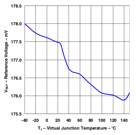
| VREF | Reference voltage | RREF = 0.39 Ω to 1 Ω | 168 | 177 | 185 | mV |
| IREF | Reference input current | VREF = 180 mV | –1 | 0.1 | 1 | μA |
| STATUS OUTPUT (ST) ELECTRICAL CHARACTERISTICS | ||||||
| VIQL | Lower status-switching threshold | ST = L | 15 | 25 | mV | |
| VIQH | Upper status-switching threshold | ST = H | 30 | 40 | mV | |
| VSTL | Low-level status voltage | IST = 1.5 mA | 0.4 | V | ||
| ISTLK | Leakage current | VST = 5 V | 5 | μA | ||
| STATUS DELAY (D) ELECTRICAL CHARACTERISTICS | ||||||
| tSTHL | Delay time, status reaction | CD = 47 nF, ST H→L | 6 | 10 | 14 | ms |
| tSTLH | Delay time, status release | CD = 47 nF, ST L→H | 10 | 20 | μs | |
(1) VQ – VREF equals the forward voltage sum of the connected LEDs (see Figure 3).
6.6 Typical Characteristics


