JAJSHO6F March 2005 – July 2019 TL431-Q1 , TL432-Q1
PRODUCTION DATA.
- 1 特長
- 2 アプリケーション
- 3 概要
- 4 改訂履歴
- 5 Pin Configuration and Functions
- 6 Specifications
- 7 Parameter Measurement Information
- 8 Detailed Description
- 9 Application and Implementation
- 10Power Supply Recommendations
- 11Layout
- 12デバイスおよびドキュメントのサポート
- 13メカニカル、パッケージ、および注文情報
パッケージ・オプション
デバイスごとのパッケージ図は、PDF版データシートをご参照ください。
メカニカル・データ(パッケージ|ピン)
- DBZ|3
サーマルパッド・メカニカル・データ
発注情報
6.8 Typical Characteristics

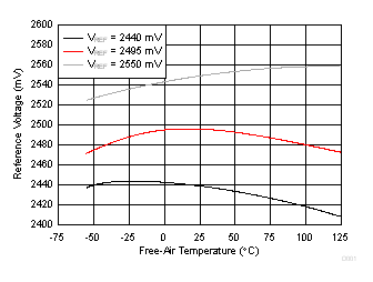
Data is for devices having the indicated value of VREF at IKA = 10 mA, TA = 25°C.
Figure 1. Reference Voltage vs Free-air Temperature  Figure 3. Cathode Current vs Cathode Voltage
  Figure 5. OFF-State Cathode Current vs
Free-air Temperature
 Figure 7. Equivalent Input Noise Voltage vs Frequency
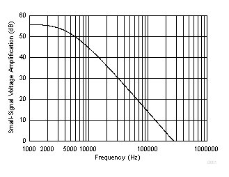
  Figure 9. Small-Signal Voltage Amplification vs Frequency

The areas under the curves represent conditions that may cause the device to oscillate. For curves B, C, and D, R2 and VREF were adjusted to establish the initial VKA and IKA conditions with CL = 0. VBATT and CL then were adjusted to determine the ranges of stability (see Figure 18 and Figure 19 for test circuits).
Figure 13. Stability Boundary Conditions for All TL43x, SOT-23, SC-70, and Q-TEMP Devices 
 Figure 4. Cathode Current vs Cathode Voltage
  Figure 6. Ratio of Delta Reference Voltage to Delta Cathode Voltage vs Free-air Temperature
  Figure 8. Equivalent Input Noise Voltage Over a 10-s Period
  Figure 10. Reference Impedance vs Frequency
The areas under the curves represent conditions that may cause the device to oscillate. For curves B, C, and D, R2 and VREF were adjusted to establish the initial VKA and IKA conditions with CL = 0. VBATT and CL then were adjusted to determine the ranges of stability (see Figure 18 and Figure 19 for test circuits).
Figure 12. Stability Boundary Conditions for All TL43x Devices (Except for SOT23-3, SC-70,
and Q-TEMP Devices)