SBAS961A May   2019  – April 2020 TLA2528

PRODUCTION DATA.  

  1. Features
  2. Applications
  3. Description
    1.     Device Images
      1.      TLA2528 Block Diagram and Applications
  4. Revision History
  5. Pin Configuration and Functions
    1.     Pin Functions
  6. Specifications
    1. 6.1      Absolute Maximum Ratings
    2. 6.2      ESD Ratings
    3. 6.3      Recommended Operating Conditions
    4. 6.4      Thermal Information
    5. 6.5      Electrical Characteristics
    6. Table 1. I2C Timing Requirements
    7. Table 2. Timing Requirements
    8. Table 3. I2C Switching Characteristics
    9. 6.6      Switching Characteristics
    10. 6.7      Typical Characteristics
  7. Detailed Description
    1. 7.1 Overview
    2. 7.2 Functional Block Diagram
    3. 7.3 Feature Description
      1. 7.3.1  Multiplexer and ADC
      2. 7.3.2  Reference
      3. 7.3.3  ADC Transfer Function
      4. 7.3.4  ADC Offset Calibration
      5. 7.3.5  I2C Address Selector
      6. 7.3.6  Programmable Averaging Filter
      7. 7.3.7  General-Purpose I/Os (GPIOs)
      8. 7.3.8  Oscillator and Timing Control
      9. 7.3.9  Output Data Format
      10. 7.3.10 I2C Protocol Features
        1. 7.3.10.1 General Call
        2. 7.3.10.2 General Call With Software Reset
        3. 7.3.10.3 General Call With a Software Write to the Programmable Part of the Slave Address
        4. 7.3.10.4 Configuring the Device for High-Speed I2C Mode
    4. 7.4 Device Functional Modes
      1. 7.4.1 Device Power-Up and Reset
      2. 7.4.2 Manual Mode
      3. 7.4.3 Auto-Sequence Mode
    5. 7.5 Programming
      1. 7.5.1 Reading Registers
        1. 7.5.1.1 Single Register Read
        2. 7.5.1.2 Reading a Continuous Block of Registers
      2. 7.5.2 Writing Registers
        1. 7.5.2.1 Single Register Write
        2. 7.5.2.2 Set Bit
        3. 7.5.2.3 Clear Bit
        4. 7.5.2.4 Writing a Continuous Block of Registers
    6. 7.6 TLA2528 Registers
      1. 7.6.1  SYSTEM_STATUS Register (Address = 0x0) [reset = 0x80]
        1. Table 13. SYSTEM_STATUS Register Field Descriptions
      2. 7.6.2  GENERAL_CFG Register (Address = 0x1) [reset = 0x0]
        1. Table 14. GENERAL_CFG Register Field Descriptions
      3. 7.6.3  DATA_CFG Register (Address = 0x2) [reset = 0x0]
        1. Table 15. DATA_CFG Register Field Descriptions
      4. 7.6.4  OSR_CFG Register (Address = 0x3) [reset = 0x0]
        1. Table 16. OSR_CFG Register Field Descriptions
      5. 7.6.5  OPMODE_CFG Register (Address = 0x4) [reset = 0x0]
        1. Table 17. OPMODE_CFG Register Field Descriptions
      6. 7.6.6  PIN_CFG Register (Address = 0x5) [reset = 0x0]
        1. Table 18. PIN_CFG Register Field Descriptions
      7. 7.6.7  GPIO_CFG Register (Address = 0x7) [reset = 0x0]
        1. Table 19. GPIO_CFG Register Field Descriptions
      8. 7.6.8  GPO_DRIVE_CFG Register (Address = 0x9) [reset = 0x0]
        1. Table 20. GPO_DRIVE_CFG Register Field Descriptions
      9. 7.6.9  GPO_VALUE Register (Address = 0xB) [reset = 0x0]
        1. Table 21. GPO_VALUE Register Field Descriptions
      10. 7.6.10 GPI_VALUE Register (Address = 0xD) [reset = 0x0]
        1. Table 22. GPI_VALUE Register Field Descriptions
      11. 7.6.11 SEQUENCE_CFG Register (Address = 0x10) [reset = 0x0]
        1. Table 23. SEQUENCE_CFG Register Field Descriptions
      12. 7.6.12 CHANNEL_SEL Register (Address = 0x11) [reset = 0x0]
        1. Table 24. CHANNEL_SEL Register Field Descriptions
      13. 7.6.13 AUTO_SEQ_CH_SEL Register (Address = 0x12) [reset = 0x0]
        1. Table 25. AUTO_SEQ_CH_SEL Register Field Descriptions
  8. Application and Implementation
    1. 8.1 Application Information
    2. 8.2 Typical Applications
      1. 8.2.1 Mixed-Channel Configuration
        1. 8.2.1.1 Design Requirements
        2. 8.2.1.2 Detailed Design Procedure
          1. 8.2.1.2.1 Digital Input
          2. 8.2.1.2.2 Digital Open-Drain Output
        3. 8.2.1.3 Application Curve
      2. 8.2.2 Digital Push-Pull Output
  9. Power Supply Recommendations
    1. 9.1 AVDD and DVDD Supply Recommendations
  10. 10Layout
    1. 10.1 Layout Guidelines
    2. 10.2 Layout Example
  11. 11Device and Documentation Support
    1. 11.1 Receiving Notification of Documentation Updates
    2. 11.2 Community Resources
    3. 11.3 Trademarks
    4. 11.4 Electrostatic Discharge Caution
    5. 11.5 Glossary
  12. 12Mechanical, Packaging, and Orderable Information

パッケージ・オプション

メカニカル・データ(パッケージ|ピン)
サーマルパッド・メカニカル・データ
発注情報

Output Data Format

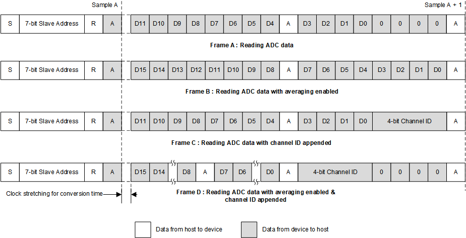
Figure 25 illustrates various I2C frames for reading data.

  • Read the ADC conversion result: Two 8-bit I2C packets are required (frame A).
  • Read the averaged conversion result: Two 8-bit I2C packets are required (frame B).
  • Read data with the channel ID appended: The 4-bit channel ID can be appended to the 12-bit ADC result by configuring the APPEND_STATUS field in the GENERAL_CFG register. When the channel ID is appended to the 12-bit ADC data, two I2C packets are required (frame C). If the channel ID is appended to the 16-bit average result, three I2C frames are required (frame D).
TLA2528 reading_adc_data_TLA7128.gifFigure 25. Data Frames for Reading Data