SGLS156F March 2003 – December 2016 TLC3702-Q1
PRODUCTION DATA.
- 1 Features
- 2 Applications
- 3 Description
- 4 Revision History
- 5 Pin Configuration and Functions
- 6 Specifications
- 7 Parameter Measurement Information
- 8 Detailed Description
- 9 Application and Implementation
- 10Power Supply Recommendations
- 11Layout
- 12Device and Documentation Support
- 13Mechanical, Packaging, and Orderable Information
パッケージ・オプション
デバイスごとのパッケージ図は、PDF版データシートをご参照ください。
メカニカル・データ(パッケージ|ピン)
- D|8
- PW|8
サーマルパッド・メカニカル・データ
発注情報
7 Parameter Measurement Information
CAUTION
The TLC3702-Q1 contains a digital output stage which, if held in the linear region of the transfer curve, can cause damage to the device.
Conventional operational amplifier and comparator testing incorporates the use of a servo loop which is designed to force the device output to a level within this linear region. Because the servo-loop method of testing cannot be used, the following alternatives are offered for measuring parameters such as input offset voltage, common-mode rejection, and so forth.
To verify that the input offset voltage falls within the limits specified, the limit value is applied to the input as shown in Figure 18(a). With the noninverting input positive with respect to the inverting input, the output should be high. With the input polarity reversed, the output should be low.
A similar test can be made to verify the input offset voltage at the common-mode extremes. The supply voltages can be slewed to provide greater accuracy, as shown in Figure 18(b) for the VICR test. This slewing is done instead of changing the input voltages.
A close approximation of the input offset voltage can be obtained by using a binary search method to vary the differential input voltage while monitoring the output state. When the applied input voltage differential is equal, but opposite in polarity, to the input offset voltage, the output changes states.
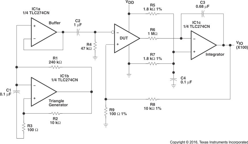
Figure 19 illustrates a practical circuit for direct dc measurement of input offset voltage that does not bias the comparator in the linear region. The circuit consists of a switching mode servo loop in which IC1a generates a triangular waveform of approximately 20-mV amplitude. IC1b acts as a buffer, with C2 and R4 removing any residual dc offset. The signal is then applied to the inverting input of the comparator under test, while the noninverting input is driven by the output of the integrator formed by IC1c through the voltage divider formed by R8 and R9. The loop reaches a stable operating point when the output of the comparator under test has a duty cycle of exactly 50%, which can only occur when the incoming triangle wave is sliced symmetrically or when the voltage at the noninverting input exactly equals the input offset voltage.
Voltage dividers R8 and R9 provide an increase in input offset voltage by a factor of 100 to make measurement easier. The values of R5, R7, R8, and R9 can significantly influence the accuracy of the reading; therefore, TI recommends that their tolerance level be one percent or lower.
Measuring the extremely low values of input current requires isolation from all other sources of leakage current and compensation for the leakage of the test socket and board. With a good picoammeter, the socket and board leakage can be measured with no device in the socket. Subsequently, this open socket leakage value can be subtracted from the measurement obtained with a device in the socket to obtain the actual input current of the device.
 Figure 18. Method for Verifying That Input Offset Voltage Is Within Specified Limits
 Figure 19. Circuit for Input Offset Voltage Measurement
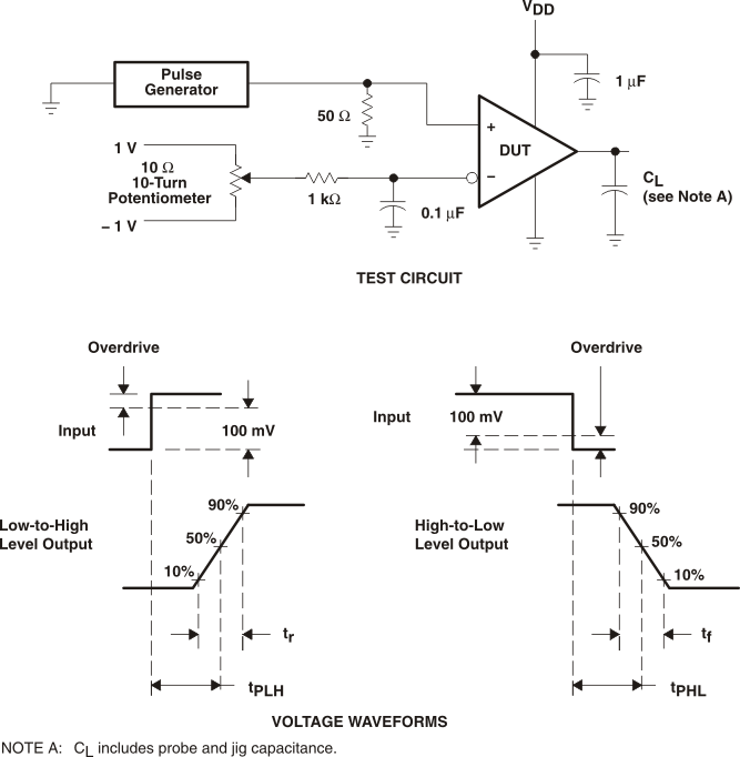
Response time is defined as the interval between the application of an input step function and the instant when the output reaches 50% of its maximum value. Response time for the low-to-high-level output is measured from the leading edge of the input pulse, while response time for the high-to-low-level output is measured from the trailing edge of the input pulse. Response time measurement at low input signal levels can be greatly affected by the input offset voltage. The offset voltage should be balanced by the adjustment at the inverting input as shown in Figure 20, so that the circuit is just at the transition point. A low signal, for example 105-mV or 5-mV overdrive, causes the output to change state
 Figure 20. Response, Rise, and Fall Times Circuit and Voltage Waveforms