SLVSCZ9A October 2015 – November 2015 TLC59581 , TLC59582
PRODUCTION DATA.
- 1 Features
- 2 Applications
- 3 Description
- 4 Revision History
- 5 Description (continued)
- 6 Pin Configuration and Functions
- 7 Specifications
- 8 Parameter Measurement Information
-
9 Detailed Description
- 9.1 Overview
- 9.2 Functional Block Diagram
- 9.3
Device Functional Modes
- 9.3.1 Brightness Control (BC) Function
- 9.3.2 Color Brightness Control (CC) Function
- 9.3.3 Select RIREF For a Given BC
- 9.3.4 Choosing BC/CC For a Different Application
- 9.3.5 LED Open Detection (LOD)
- 9.3.6 Internal Circuit for Caterpillar Removal
- 9.3.7 Power Save Mode (PSM)
- 9.3.8 Internal Pre-Charge FET
- 9.3.9 Thermal Shutdown (TSD)
- 9.3.10 IREF Resistor Short Protection (ISP)
- 10Application and Implementation
- 11Power Supply Recommendations
- 12Layout
- 13Device and Documentation Support
- 14Mechanical, Packaging, and Orderable Information
1 Features
- 48 Constant-Current Sink Output Channels
- Sink Current Capability with Max BC/CC data:
- 25 mA at 5 VCC
- 20 mA at 3.3 VCC
- Global Brightness Control (BC): 3-Bit (8-Step)
- Color Brightness Control (CC) for Each Color
Group: 9-Bit (512-Step), Three Groups - LED Power Supply Voltage Up To 10 V
- VCC = 3.0 V to 5.5 V
- Constant Current Accuracy
- Channel-to-Channel = ±1%(Typ), ±3%(Max)
- Device-to-Device = ±1%(Typ), ±2%(Max)
- Data Transfer Rate: 25 MHz
- Gray Scale Clock: 33 MHz
- Pre-Charge FET to Avoid Ghosting Phenomenon
- Enhanced Circuit for Caterpillar Cancelling
- Low-Grayscale Enhancement
- LED Open Detection (LOD)
- Thermal Shut Down (TSD)
- Operating Temperature: –40°C to 85°C
2 Applications
- LED Video Displays with Multiplexing System
- LED Signboards with Multiplexing system
- High Refresh Rate & High Density LED Panel
3 Description
The TLC59581/82are 48-channel constant-current sink drivers. Each channel has an individually-adjustable, 65536-step, pulse width modulation (PWM) grayscale (GS) brightness control.
The TLC59581 can support 32-multiplexing while TLC59582 can support 16-multiplexing.
The output channels are divided into three groups. Each group has a 512-step color brightness control (CC). CC adjusts brightness control between colors. The maximum current value of all 48 channels can be set by 8-step global brightness control (BC). BC adjusts brightness deviation between LED drivers. GS, CC and BC data are accessible through a serial interface port.
See application note Build High Density, High Refresh Rate, Multiplexing LED Panel with TLC59581, SLVA744.
Device Information(1)
| PART NUMBER | PACKAGE | BODY SIZE (NOM) |
|---|---|---|
| TLC59581 | VQFN (56) | 8.00 mm × 8.00 mm |
| TLC59582 |
- For all available packages, see the orderable addendum at the end of the data sheet.
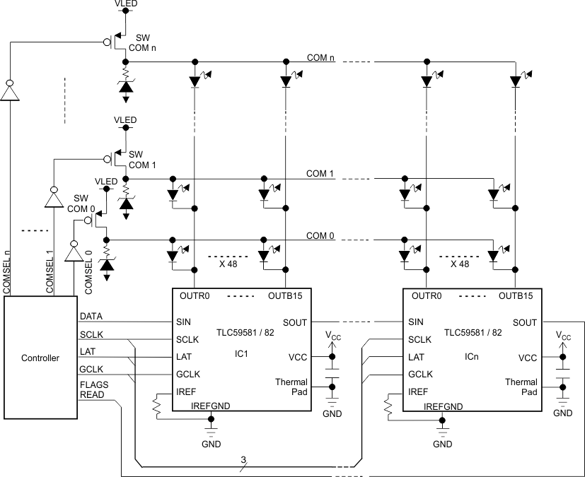
Typical Application Schematic (Multiple Daisy-Chained TLC59581/82)
