JAJSNK8D November   2021  – July 2022 TLC6984

PRODUCTION DATA  

  1. 特長
  2. アプリケーション
  3. 概要
  4. Revision History
  5. 概要 (続き)
  6. Pin Configuration and Functions
  7. Specifications
    1. 7.1 Absolute Maximum Ratings
    2. 7.2 ESD Ratings
    3. 7.3 Recommended Operating Conditions
    4. 7.4 Thermal Information
    5. 7.5 Electrical Characteristics
    6. 7.6 Timing Requirements
    7. 7.7 Switching Characteristics
    8. 7.8 Typical Characteristics
  8. Detailed Description
    1. 8.1 Overview
    2. 8.2 Functional Block Diagram
    3. 8.3 Feature Description
      1. 8.3.1 Independent and Stackable Mode
        1. 8.3.1.1 Independent Mode
        2. 8.3.1.2 Stackable Mode
      2. 8.3.2 Current Setting
        1. 8.3.2.1 Brightness Control (BC) Function
        2. 8.3.2.2 Color Brightness Control (CC) Function
        3. 8.3.2.3 Choosing BC/CC for a Different Application
      3. 8.3.3 Frequency Multiplier
      4. 8.3.4 Line Transitioning Sequence
      5. 8.3.5 Protections and Diagnostics
        1. 8.3.5.1 Thermal Shutdown Protection
        2. 8.3.5.2 IREF Resistor Short Protection
        3. 8.3.5.3 LED Open Load Detection and Removal
          1. 8.3.5.3.1 LED Open Detection
          2. 8.3.5.3.2 Read LED Open Information
          3. 8.3.5.3.3 LED Open Caterpillar Removal
        4. 8.3.5.4 LED Short and Weak Short Circuitry Detection and Removal
          1. 8.3.5.4.1 LED Short and Weak Short Detection
          2. 8.3.5.4.2 Read LED Short Information
          3. 8.3.5.4.3 LSD Caterpillar Removal
    4. 8.4 Device Functional Modes
    5. 8.5 Continuous Clock Series Interface
      1. 8.5.1 Data Validity
      2. 8.5.2 CCSI Frame Format
      3. 8.5.3 Write Command
        1. 8.5.3.1 Chip Index Write Command
        2. 8.5.3.2 VSYNC Write Command
        3. 8.5.3.3 MPSM Write Command
        4. 8.5.3.4 Standby Clear and Enable Command
        5. 8.5.3.5 Soft_Reset Command
        6. 8.5.3.6 Data Write Command
      4. 8.5.4 Read Command
    6. 8.6 PWM Grayscale Control
      1. 8.6.1 Grayscale Data Storage and Display
        1. 8.6.1.1 Memory Structure Overview
        2. 8.6.1.2 Details of Memory Bank
        3. 8.6.1.3 Write a Frame Data into Memory Bank
      2. 8.6.2 PWM Control for Display
    7. 8.7 Register Maps
      1. 8.7.1  FC0
      2. 8.7.2  FC1
      3. 8.7.3  FC2
      4. 8.7.4  FC3
      5. 8.7.5  FC4
      6. 8.7.6  FC14
      7. 8.7.7  FC15
      8. 8.7.8  FC16
      9. 8.7.9  FC17
      10. 8.7.10 FC18
      11. 8.7.11 FC19
      12. 8.7.12 FC20
      13. 8.7.13 FC21
  9. Application and Implementation
    1. 9.1 Application Information
    2. 9.2 Typical Application
      1. 9.2.1 Design Requirements
        1. 9.2.1.1 System Structure
        2. 9.2.1.2 SCLK Frequency
        3. 9.2.1.3 Internal GCLK Frequency
        4. 9.2.1.4 Line Switch Time
        5. 9.2.1.5 Blank Time Removal
        6. 9.2.1.6 BC and CC
      2. 9.2.2 Detailed Design Procedure
        1. 9.2.2.1 Chip Index Command
        2. 9.2.2.2 FC Registers Settings
        3. 9.2.2.3 Grayscale Data Write
        4. 9.2.2.4 VSYNC Command
        5. 9.2.2.5 LED Open and Short Read
      3. 9.2.3 Application Curves
  10. 10Power Supply Recommendations
  11. 11Layout
    1. 11.1 Layout Guidelines
    2. 11.2 Layout Example
  12. 12Device and Documentation Support
    1. 12.1 Documentation Support
      1. 12.1.1 Related Documentation
    2. 12.2 Receiving Notification of Documentation Updates
    3. 12.3 サポート・リソース
    4. 12.4 Trademarks
    5. 12.5 Electrostatic Discharge Caution
    6. 12.6 Glossary
  13. 13Mechanical, Packaging, and Orderable Information

パッケージ・オプション

メカニカル・データ(パッケージ|ピン)
サーマルパッド・メカニカル・データ
発注情報

Detailed Design Procedure

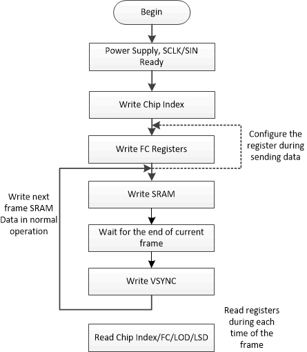
Figure 9-3 gives a detail design procedure for LED display. After power on and digital signals are ready, the first step for the controller is to send the chip index command to let the devices know their identifications. Then, the controller sends the configuration data to the FC registers. After this, it sends the VSYNC at the beginning of each frame and also sends the data to each device. The devices display the data of last frame when the VSYNC comes and meanwhile receive the data of current frame transmitted from controller. The registers can be read at anytime of the frame.
GUID-978C2928-8937-4880-9F0F-9422833FDD9A-low.gifFigure 9-3 Design Procedure for LED Display