JAJSC76 May 2016 TLC6C5912
PRODUCTION DATA.
8 Detailed Description
8.1 Overview
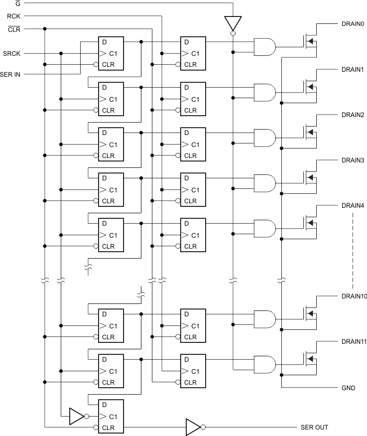
The TLC6C5912 device is a monolithic, medium-voltage, low current 12-bit shift register designed to drive relatively moderate load power such LEDs. The device contains a 12-bit serial-in, parallel-out shift register that feeds a 12-bit D-type storage register. Thermal shutdown protection is also built-into the device.
8.2 Functional Block Diagram

8.3 Feature Description
8.3.1 Thermal Shutdown
The device implements an internal thermal shutdown to protect itself if the junction temperature exceeds 175°C (typical). The thermal shutdown forces the device to have an open state when the junction temperature exceeds the thermal trip threshold. Once the junction temperature decreases to less than 160°C (typical), the device begins to operate again.
8.3.2 Serial-In Interface
The TLC6C598 device contains an 8-bit serial-in, parallel out shift register that feeds an 8-bit D-type storage register. Data transfer through both the shift and storage registers on the rising edge of the shift register clock (SRCK) and the register clock (RCK), respectively. The storage transfers data to the output buffer when shift register clear (CLR) is high.
8.3.3 Clear Register
A logic low on CLR clears all registers in the device. TI suggests clearing the device during power up or initialization.
8.3.4 Cascade Through SER OUT
By connecting the SER OUT pin to the SER IN input of the next device on the serial bus to cascade, the data transfers to the next device on the falling edge of SRCK. This can improve the cascade application reliability, as it can avoid that the second device receives SRCK and data input at the same rising edge of SRCK.
8.3.5 Output Control
Holding the output enable (G) high holds all data in the output buffers low, and all drain outputs are off. Holding G low makes data from the storage register transparent to the output buffers. When data in the output buffers is low, the DMOS transistor outputs are off. When data is high, the DMOS transistor outputs are capable of sink-current. This pin also be used for global PWM dimming.
8.4 Device Functional Modes
8.4.1 Operation With VCC < 3 V
This device works normally during 3 V ≤ VCC ≤ 5.5 V, when operation voltage is lower than 3 V. The behavior of device cannot be ensured, including communication interface and current capability.
8.4.2 Operation With 5.5 V ≤ VCC ≤ 8 V
The device works normally during this voltage range, but reliability issues may occurs while the device works for a long time in this voltage range.