SLVS647I August 2006 – November 2014 TLE4275-Q1
UNLESS OTHERWISE NOTED, this document contains PRODUCTION DATA.
- 1 Features
- 2 Applications
- 3 Description
- 4 Revision History
- 5 Pin Configuration and Functions
- 6 Specifications
- 7 Parameter Measurement Information
- 8 Detailed Description
- 9 Application and Implementation
- 10Power Supply Recommendations
- 11Layout
- 12Device and Documentation Support
- 13Mechanical, Packaging, and Orderable Information
パッケージ・オプション
デバイスごとのパッケージ図は、PDF版データシートをご参照ください。
メカニカル・データ(パッケージ|ピン)
- KTT|5
- PWP|20
- KVU|5
サーマルパッド・メカニカル・データ
発注情報
1 Features
2 Applications
- Qualified for Automotive Applications
- Cluster
- Body Control Modules
- Heating Ventilation and Air Conditioning (HVAC)
3 Description
The TLE4275-Q1 is a monolithic integrated low-dropout voltage regulator offered in a 5-pin TO package. The device regulates an input voltage up to 45 V to VOUT = 5 V (typical). The device can drive loads up to 450 mA and is short-circuit proof. At overtemperature, the incorporated temperature protection turns off the TLE4275-Q1. The device generates a reset signal for an output voltage, VOUT,rt, of 4.65 V (typical). By the use of an external delay capacitor, one can program the reset delay time.
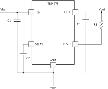
The input capacitor, CIN, compensates for line fluctuation. Using a resistor of approximately 1 Ω in series with CIN dampens the oscillation of input inductance and input capacitance. The output capacitor, COUT, stabilizes the regulation circuit. The specification for stability is at COUT ≥ 22 μF and ESR ≤ 5 Ω, within the operating temperature range. Stability for electrolytic capacitors specifically is at COUT ≥ 68 µF within the operating temperature range. See the application report on low-temperature stability, SLVA501, for further details.
The control amplifier compares a reference voltage to a voltage that is proportional to the output voltage and drives the base of the series transistor through a buffer. Saturation control as a function of the load current prevents any oversaturation of the power element. The device also incorporates a number of internal circuits for protection against: overload, overtemperature, and reverse polarity.
Device Information(1)
| PART NUMBER | PACKAGE | BODY SIZE (NOM) |
|---|---|---|
| TLE4275-Q1 | DDPAK/TO-263 (5) | 10.16 mm × 8.42 mm |
| TO-252 (5) | 6.10 mm × 6.60 mm | |
| HTSSOP (20) | 6.50 mm × 4.40 mm |
- For all available packages, see the orderable addendum at the end of the data sheet.
Typical Application
