JAJSK64A March   2021  – April 2022 TLIN2021A-Q1

PRODMIX  

  1. 特長
  2. アプリケーション
  3. 概要
  4. Revision History
  5. 概要 (続き)
  6. Pin Configuration and Functions
  7. Specification
    1. 7.1 Absolute Maximum Ratings
    2. 7.2 ESD Ratings
    3. 7.3 ESD Ratings - IEC Specification
    4. 7.4 Thermal Information
    5. 7.5 Recommended Operating Conditions
    6. 7.6 Power Supply Characteristics
    7. 7.7 Electrical Characteristics
    8. 7.8 AC Switching Characteristics
    9. 7.9 Typical Curves
  8. Parameter Measurement Information
  9. Detailed Description
    1. 9.1 Overview
    2. 9.2 Functional Block Diagram
    3. 9.3 Feature Description
      1. 9.3.1  LIN
        1. 9.3.1.1 LIN Transmitter Characteristics
        2. 9.3.1.2 LIN Receiver Characteristics
          1. 9.3.1.2.1 Termination
      2. 9.3.2  TXD
      3. 9.3.3  RXD
      4. 9.3.4  VSUP
      5. 9.3.5  GND
      6. 9.3.6  EN
      7. 9.3.7  WAKE
      8. 9.3.8  INH
      9. 9.3.9  Local Faults
      10. 9.3.10 TXD Dominant Time-Out (DTO)
      11. 9.3.11 Bus Stuck Dominant System Fault: False Wake-Up Lockout
      12. 9.3.12 Thermal Shutdown
      13. 9.3.13 Under Voltage on VSUP
      14. 9.3.14 Unpowered Device
    4. 9.4 Device Functional Modes
      1. 9.4.1 Normal Mode
      2. 9.4.2 Sleep Mode
      3. 9.4.3 Standby Mode
      4. 9.4.4 Wake-Up Events
        1. 9.4.4.1 Local Wake-Up (LWU) via WAKE Input Terminal
        2. 9.4.4.2 Wake-Up Request (RXD)
  10. 10Application Information Disclaimer
    1. 10.1 Application Information
    2. 10.2 Typical Application
      1. 10.2.1 Design Requirements
      2. 10.2.2 Detailed Design Procedures
        1. 10.2.2.1 Normal Mode Application Note
        2. 10.2.2.2 TXD Dominant State Time-Out Application Note
        3. 10.2.2.3 Standby Mode Application Note
      3. 10.2.3 Application Curves
  11. 11Power Supply Recommendations
  12. 12Layout
    1. 12.1 Layout Guidelines
    2. 12.2 Layout Example
  13. 13Device and Documentation Support
    1. 13.1 Documentation Support
    2. 13.2 Receiving Notification of Documentation Updates
    3. 13.3 サポート・リソース
    4. 13.4 Trademarks
    5. 13.5 Electrostatic Discharge Caution
    6. 13.6 Glossary
  14. 14Mechanical, Packaging, and Orderable Information

パッケージ・オプション

メカニカル・データ(パッケージ|ピン)
サーマルパッド・メカニカル・データ
発注情報

Application Curves

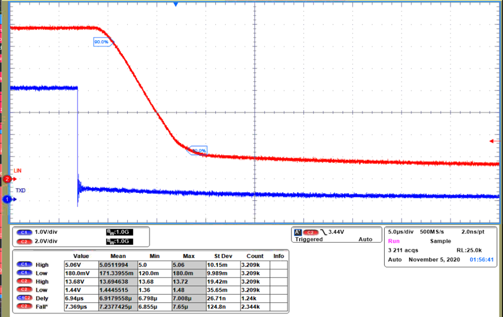
Figure 10-2 and Figure 10-3 show the propagation delay from the TXD pin to the LIN pin for the dominant to recessive and recessive to dominant edges. Device was configured in commander mode with external pull-up resistor (1 kΩ) and 680 pF bus capacitance.
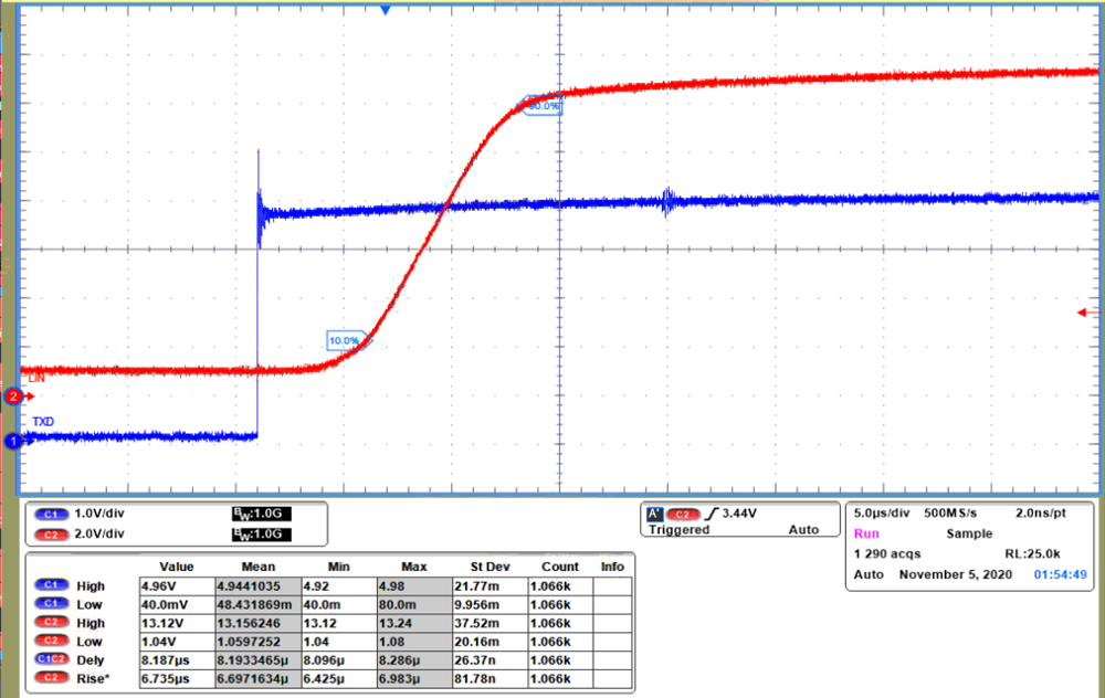
GUID-20201208-CA0I-P3LT-WWCZ-5KQRSCKD15J8-low.pngFigure 10-2 Dominant To Recessive Propagation Delay
GUID-20201208-CA0I-DKBK-FQNH-ZLR7SZPFTLZC-low.pngFigure 10-3 Recessive to Dominant Propagation Delay