JAJSE11B November 2015 – September 2017 TLV1701-Q1 , TLV1702-Q1 , TLV1704-Q1
PRODUCTION DATA.
- 1 特長
- 2 アプリケーション
- 3 概要
- 4 改訂履歴
- 5 Device Comparison Table
- 6 Pin Configuration and Functions
- 7 Specifications
- 8 Detailed Description
- 9 Application and Implementation
- 10Power Supply Recommendations
- 11Layout
- 12デバイスおよびドキュメントのサポート
- 13メカニカル、パッケージ、および注文情報
パッケージ・オプション
メカニカル・データ(パッケージ|ピン)
サーマルパッド・メカニカル・データ
発注情報
7 Specifications
7.1 Absolute Maximum Ratings
over operating free-air temperature range (unless otherwise noted)(1)| MIN | MAX | UNIT | ||
|---|---|---|---|---|
| Supply voltage | 40 (±20) | V | ||
| Signal input pins | Voltage(2) | (VS–) – 0.5 | (VS+) + 0.5 | V |
| Current(2) | ±10 | mA | ||
| Output short-circuit(3) | Continuous | mA | ||
| Operating temperature | –55 | 150 | °C | |
| Junction temperature, TJ | 150 | °C | ||
| Storage temperature, Tstg | –65 | 150 | °C | |
(1) Stresses beyond those listed under Absolute Maximum Ratings may cause permanent damage to the device. These are stress ratings only, and functional operation of the device at these or any other conditions beyond those indicated under Recommended Operating Conditions is not implied. Exposure to absolute-maximum-rated conditions for extended periods may affect device reliability.
(2) Input pins are diode-clamped to the power-supply rails. Input signals that can swing more than 0.5 V beyond the supply rails must be current limited to 10 mA or less.
(3) Short-circuit to ground; one comparator per package.
7.2 ESD Ratings
| VALUE | UNIT | |||
|---|---|---|---|---|
| TLV1701-Q1 | ||||
| V(ESD) | Electrostatic discharge | Human-body model (HBM), per AEC Q100-002(1) | ±2000 | V |
| Charged-device model (CDM), per AEC Q100-011 | ±1000 | |||
| TLV1702-Q1 | ||||
| V(ESD) | Electrostatic discharge | Human-body model (HBM), per AEC Q100-002(1) | ±1000 | V |
| Charged-device model (CDM), per AEC Q100-011 | ±1000 | |||
| TLV1704-Q1 | ||||
| V(ESD) | Electrostatic discharge | Human-body model (HBM), per AEC Q100-002(1) | ±1000 | V |
| Charged-device model (CDM), per AEC Q100-011 | ±1000 | |||
(1) AEC Q100-002 indicates that HBM stressing shall be in accordance with the ANSI/ESDA/JEDEC JS-001 specification.
7.3 Recommended Operating Conditions
over operating free-air temperature range (unless otherwise noted)| MIN | NOM | MAX | UNIT | ||
|---|---|---|---|---|---|
| Supply voltage VS = (VS+) – (VS–) | 2.2 (±1.1) | 36 (±18) | V | ||
| Specified temperature | –40 | 125 | °C | ||
7.4 Thermal Information
| THERMAL METRIC(1) | TLV1701-Q1 | TLV1702-Q1 | TLV1704-Q1 | UNIT | |
|---|---|---|---|---|---|
| DBV (SOT-23) | DGK (VSSOP) | PW (TSSOP) | |||
| 5 PINS | 8 PINS | 14 PINS | |||
| RθJA | Junction-to-ambient thermal resistance | 233.1 | 199 | 128.1 | °C/W |
| RθJC(top) | Junction-to-case (top) thermal resistance | 156.4 | 89.5 | 56.5 | °C/W |
| RθJB | Junction-to-board thermal resistance | 60.6 | 120.4 | 69.9 | °C/W |
| ψJT | Junction-to-top characterization parameter | 35.7 | 22 | 9.1 | °C/W |
| ψJB | Junction-to-board characterization parameter | 59.7 | 118.7 | 69.3 | °C/W |
| RθJC(bot) | Junction-to-case (bottom) thermal resistance | N/A | N/A | N/A | °C/W |
(1) For more information about traditional and new thermal metrics, see the Semiconductor and IC Package Thermal Metrics application report.
7.5 Electrical Characteristics
at TA = 25°C, VS = 2.2 V to 36 V, CL = 15 pF, RPULLUP = 5.1 kΩ, VCM = VS / 2, and VS = VPULLUP (unless otherwise noted)| PARAMETER | TEST CONDITIONS | MIN | TYP | MAX | UNIT | ||
|---|---|---|---|---|---|---|---|
| OFFSET VOLTAGE | |||||||
| VOS | Input offset voltage | TA = 25°C, VS = 2.2 V | ±0.5 | ±3.5 | mV | ||
| TA = 25°C, VS = 36 V | ±0.3 | ±2.5 | mV | ||||
| TA = –40°C to +125°C | ±5.5 | mV | |||||
| TA = 25°C, VS = 36 V, TLV1701-Q1 Only | ±0.4 | ±3.2 | |||||
| TA = –40°C to +125°C, TLV1701-Q1 Only | ±6.3 | ||||||
| dVOS/dT | Input offset voltage drift | TA = –40°C to +125°C | ±4 | ±20 | μV/°C | ||
| PSRR | Power-supply rejection ratio | TA = 25°C | 15 | 100 | μV/V | ||
| TA = –40°C to +125°C | 20 | μV/V | |||||
| INPUT VOLTAGE RANGE | |||||||
| VCM | Common-mode voltage range | TA = –40°C to +125°C | (V–) | (V+) | V | ||
| INPUT BIAS CURRENT | |||||||
| IB | Input bias current | TA = 25°C | 5 | 15 | nA | ||
| TA = –40°C to +125°C | 20 | nA | |||||
| IOS | Input offset current | 0.5 | nA | ||||
| CLOAD | Capacitive load drive | See Typical Characteristics | |||||
| OUTPUT | |||||||
| VO | Voltage output swing from rail | IO ≤ 4 mA, input overdrive = 100 mV, VS = 36 V |
900 | mV | |||
| IO = 0 mA, input overdrive = 100 mV, VS = 36 V |
600 | mV | |||||
| ISC | Short circuit sink current | 20 | mA | ||||
| Output leakage current | VIN+ > VIN– | 70 | nA | ||||
| POWER SUPPLY | |||||||
| VS | Specified voltage range | 2.2 | 36 | V | |||
| IQ | Quiescent current (per channel) | IO = 0 A | 55 | 75 | μA | ||
| IO = 0 A, TA = –40°C to +125°C | 100 | μA | |||||
7.6 Switching Characteristics
at TA = 25°C, VS = +2.2 V to +36 V, CL = 15 pF, RPULLUP = 5.1 kΩ, VCM = VS / 2, and VS = VPULLUP (unless otherwise noted)| PARAMETER | TEST CONDITIONS | MIN | TYP | MAX | UNIT | |
|---|---|---|---|---|---|---|
| tpHL | Propagation delay time, high-to-low | Input overdrive = 100 mV | 460 | ns | ||
| tpLH | Propagation delay time, low-to-high | Input overdrive = 100 mV | 560 | ns | ||
| tR | Rise time | Input overdrive = 100 mV | 365 | ns | ||
| tF | Fall time | Input overdrive = 100 mV | 240 | ns | ||
7.7 Typical Characteristics
at TA = 25°C, VS = 5 V, RPULLUP = 5.1 kΩ, and input overdrive = 100 mV (unless otherwise noted)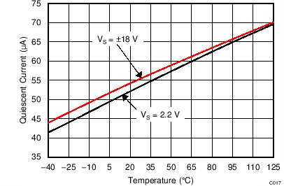
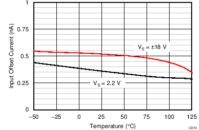
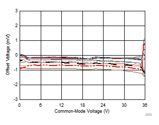
| VS = ±18 V | 14 typical units shown | |
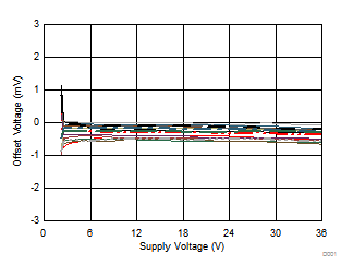
| 16 typical units shown | ||
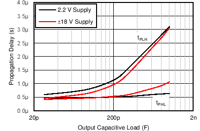
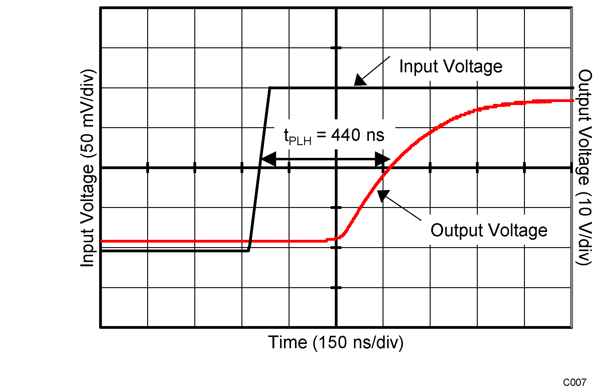
| VS = 36 V | Overdrive = 100 mV | |
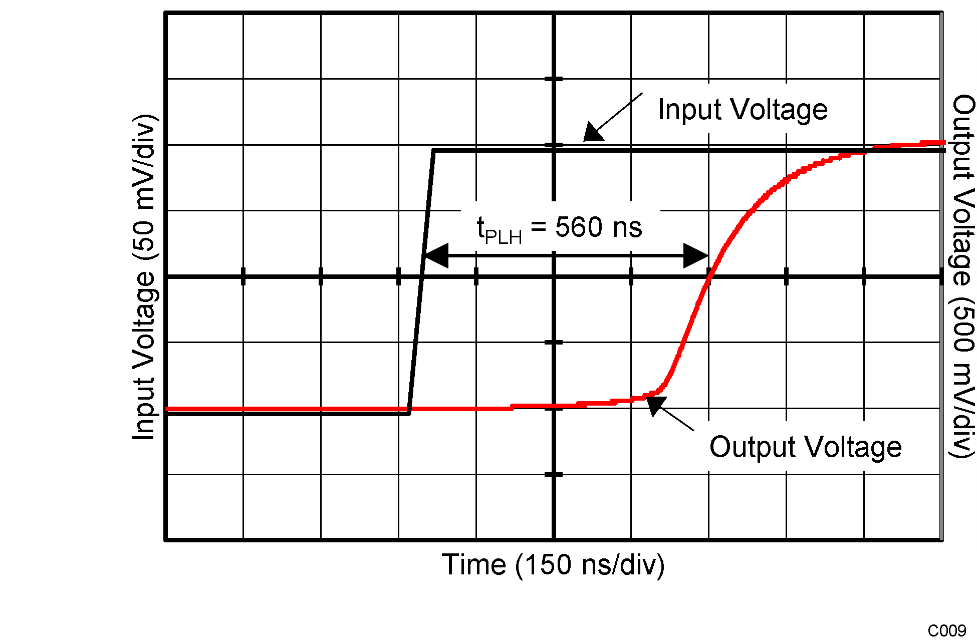
| VS = 2.2 V | Overdrive = 100 mV | |
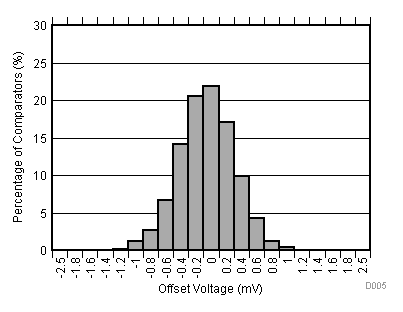
| VS = ±18 V | Distribution taken from 2524 comparators | |
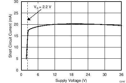
| Sink current | ||
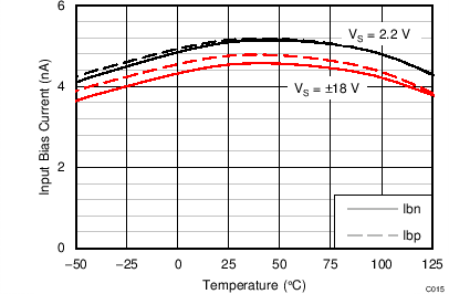
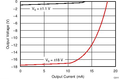
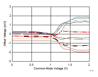
| VS = 2.2 V | 13 typical units shown | |
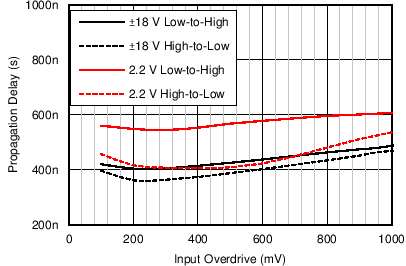
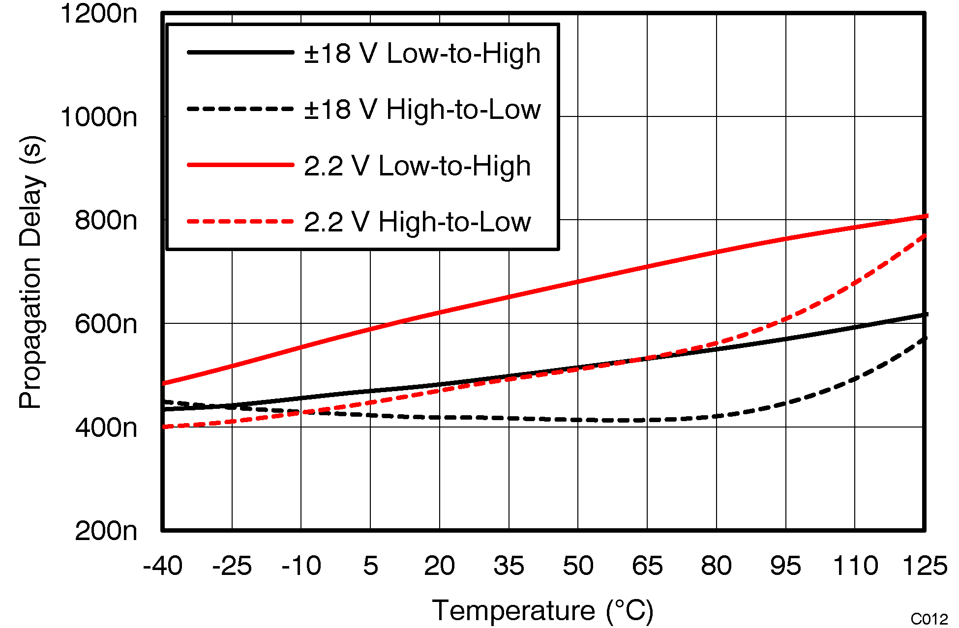
| VOD = 100 mV | ||
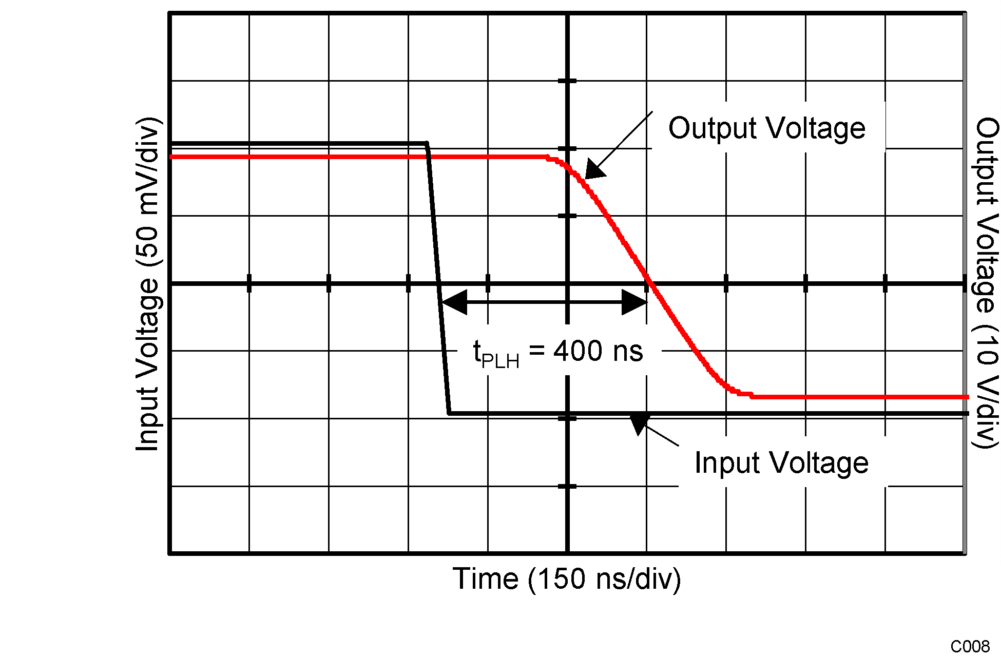
| VS = 36 V | Overdrive = 100 mV | |
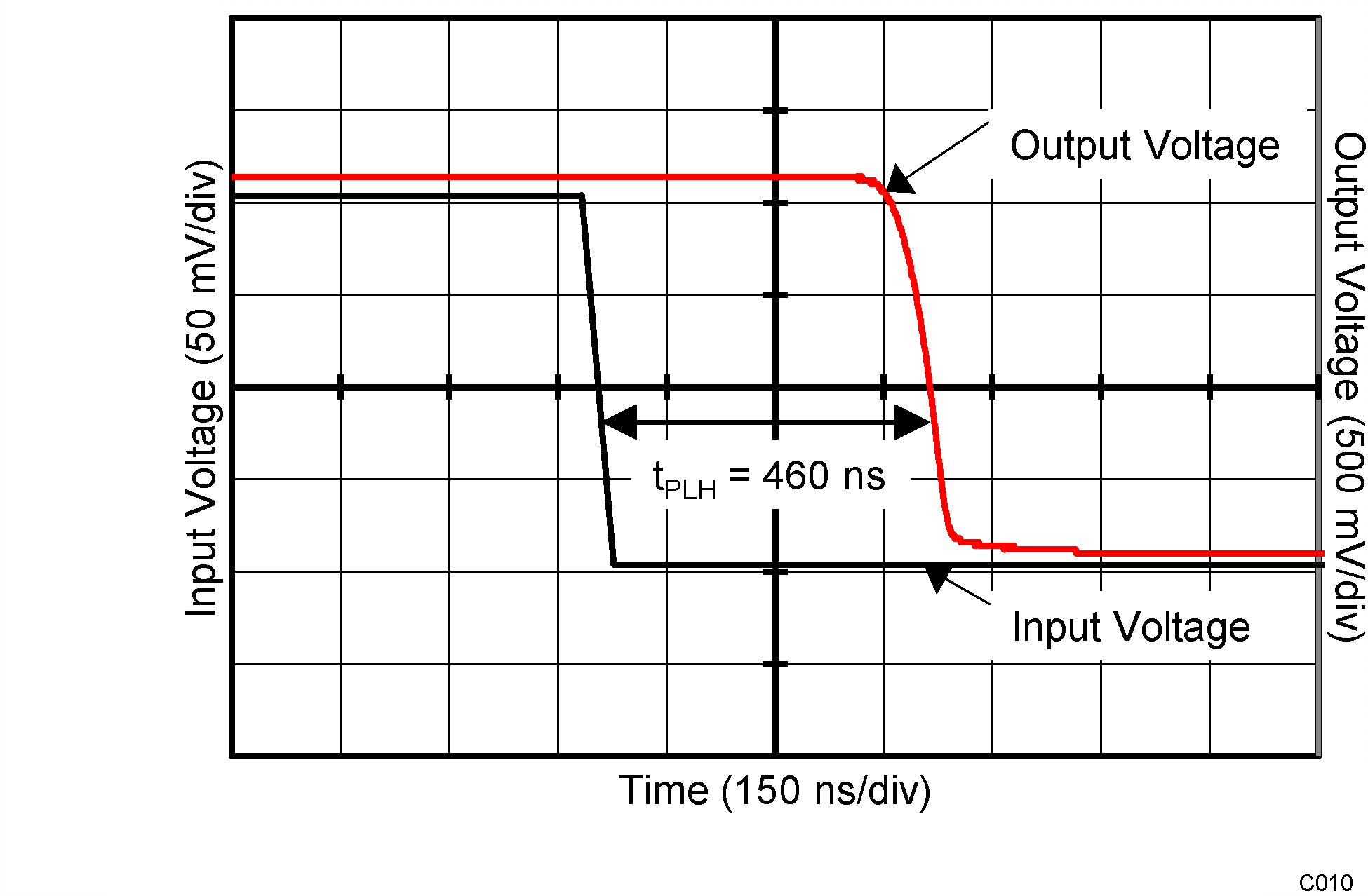
| VS = 2.2 V | Overdrive = 100 mV | |
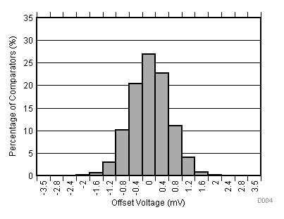
| VS = 2.2 V | Distribution taken from 2524 comparators | |