JAJSE11B November 2015 – September 2017 TLV1701-Q1 , TLV1702-Q1 , TLV1704-Q1
PRODUCTION DATA.
- 1 特長
- 2 アプリケーション
- 3 概要
- 4 改訂履歴
- 5 Device Comparison Table
- 6 Pin Configuration and Functions
- 7 Specifications
- 8 Detailed Description
- 9 Application and Implementation
- 10Power Supply Recommendations
- 11Layout
- 12デバイスおよびドキュメントのサポート
- 13メカニカル、パッケージ、および注文情報
パッケージ・オプション
メカニカル・データ(パッケージ|ピン)
サーマルパッド・メカニカル・データ
発注情報
8 Detailed Description
8.1 Overview
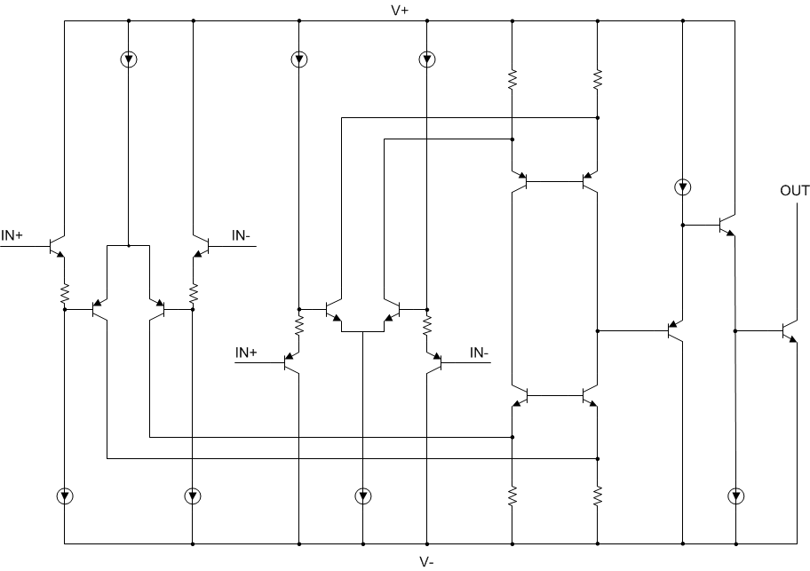
The TLV170x-Q1 comparator features rail-to-rail input and output on supply voltages as high as 36 V. The rail-to-rail input stage enables detection of signals close to the supply and ground. The open-collector configuration allows the device to be used in wired-OR configurations, such as a window comparator. A low supply current of 55 μA per channel with small, space-saving packages, makes these comparators versatile for use in a wide range of applications, from portable to industrial.
8.2 Functional Block Diagram

8.3 Feature Description
8.3.1 Comparator Inputs
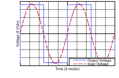
The TLV170x-Q1 device is a rail-to-rail input comparator, with an input common-mode range that includes the supply rails. The TLV170x-Q1 device is designed to prevent phase inversion when the input pins exceed the supply voltage. Figure 18 shows the TLV170x-Q1 device response when input voltages exceed the supply, resulting in no phase inversion.
 Figure 18. No Phase Inversion: Comparator Response to Input Voltage
(Propagation Delay Included)
8.4 Device Functional Modes
8.4.1 Setting Reference Voltage
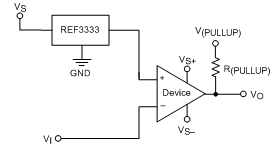
Using a stable reference is important when setting the transition point for the TLV170x-Q1 device. The REF3333, as shown in Figure 19, provides a 3.3-V reference voltage with low drift and only 3.9 μA of quiescent current.
 Figure 19. Reference Voltage for the TLV170x-Q1