JAJSGH6B November   2018  – August 2024 TLV1704-SEP

PRODUCTION DATA  

  1.   1
  2. 特長
  3. アプリケーション
  4. 概要
  5. Pin Configuration and Functions
  6. Specifications
    1. 5.1 Absolute Maximum Ratings
    2. 5.2 ESD Ratings
    3. 5.3 Recommended Operating Conditions
    4. 5.4 Thermal Information
    5. 5.5 Electrical Characteristics
    6. 5.6 Switching Characteristics
    7. 5.7 Typical Characteristics
  7. Detailed Description
    1. 6.1 Overview
    2. 6.2 Functional Block Diagram
    3. 6.3 Feature Description
      1. 6.3.1 Comparator Inputs
      2.      19
    4. 6.4 Device Functional Modes
      1. 6.4.1 Setting Reference Voltage
  8. Application and Implementation
    1. 7.1 Application Information
    2. 7.2 Typical Application
      1. 7.2.1 Design Requirements
      2. 7.2.2 Detailed Design Procedure
      3. 7.2.3 Application Curve
    3. 7.3 Power Supply Recommendations
    4. 7.4 Layout
      1. 7.4.1 Layout Guidelines
      2. 7.4.2 Layout Example
  9. Device and Documentation Support
    1. 8.1 Documentation Support
      1. 8.1.1 Related Documentation
    2. 8.2 ドキュメントの更新通知を受け取る方法
    3. 8.3 サポート・リソース
    4. 8.4 Trademarks
    5. 8.5 静電気放電に関する注意事項
    6. 8.6 用語集
  10. Revision History
  11. 10Mechanical, Packaging, and Orderable Information

パッケージ・オプション

メカニカル・データ(パッケージ|ピン)
サーマルパッド・メカニカル・データ
発注情報

Comparator Inputs

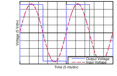
The TLV1704-SEP device is a rail-to-rail input comparator, with an input common-mode range that includes the supply rails. The TLV1704-SEP device is designed to prevent phase inversion when the input pins exceed the supply voltage. Figure 6-1 shows the TLV1704-SEP device response when input voltages exceed the supply, resulting in no phase inversion.
TLV1704-SEP No Phase Inversion: Comparator Response to Input Voltage (Propagation Delay Included)Figure 6-1 No Phase Inversion: Comparator Response to Input Voltage (Propagation Delay Included)