JAJSJP5C September 2022 – September 2023 TLV1811 , TLV1812 , TLV1814 , TLV1821 , TLV1822 , TLV1824
PRODMIX
- 1
- 1 特長
- 2 アプリケーション
- 3 概要
- 4 Revision History
- 5 Pin Configuration and Functions
- 6 Specifications
- 7 Typical Characteristics
- 8 Detailed Description
-
9 Application and Implementation
- 9.1 Application Information
- 9.2 Typical Applications
- 9.3 Power Supply Recommendations
- 9.4 Layout
- 10Device and Documentation Support
- 11Mechanical, Packaging, and Orderable Information
パッケージ・オプション
メカニカル・データ(パッケージ|ピン)
サーマルパッド・メカニカル・データ
発注情報
Pin Functions: TLV1814 and TLV1824
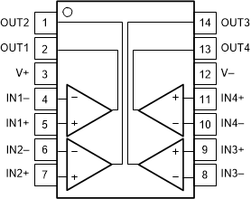
 D, PW, DYY Package, 14-Pin SOIC, TSSOP, SOT-23, Top View
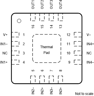
NOTE: Connect exposed thermal pad directly to V- pin.
RTE Package, 16-Pad WQFN With Exposed Thermal Pad, Top ViewTable 5-3 Pin Functions: TLV1814 and TLV1824
| PIN | I/O | DESCRIPTION | ||
|---|---|---|---|---|
| NAME | SOIC | WQFN | ||
| OUT2(1) | 1 | 15 |
O |
Output pin of the comparator 2 |
| OUT1(1) | 2 | 16 | O | Output pin of the comparator1 |
|
V+ |
3 | 1 | — | Positive supply |
| IN1– | 4 | 2 | I | Negative input pin of the comparator 1 |
| IN1+ | 5 | 4 | I | Positive input pin of the comparator 1 |
| IN2– | 6 | 5 | I | Negative input pin of the comparator 2 |
| IN2+ | 7 | 6 | I | Positive input pin of the comparator 2 |
| IN3– | 8 | 7 | I | Negative input pin of the comparator 3 |
| IN3+ | 9 | 8 | I | Positive input pin of the comparator 3 |
| IN4– | 10 | 9 | I | Negative input pin of the comparator 4 |
| IN4+ | 11 | 11 | I | Positive input pin of the comparator 4 |
| V- | 12 | 12 | — | Negative supply |
| OUT4 | 13 | 13 | O | Output pin of the comparator 4 |
| OUT3 | 14 | 14 | O | Output pin of the comparator 3 |
| NC | — | 3 | — | No Internal Connection - Leave floating or GND |
| NC | — | 10 | — | No Internal Connection - Leave floating or GND |
| Thermal Pad | — | PAD | — | Connect directly to V- pin. |
(1) Some manufacturers transpose the names of channels 1 and 2. Electrically the
pinouts are identical, just a difference in channel naming convention.