JAJSJP5C September   2022  – September 2023 TLV1811 , TLV1812 , TLV1814 , TLV1821 , TLV1822 , TLV1824

PRODMIX  

  1.   1
  2. 特長
  3. アプリケーション
  4. 概要
  5. Revision History
  6. Pin Configuration and Functions
    1.     Pin Functions: TLV18x1 and TLV18x1L
    2.     Pin Functions: TLV1812 and TLV1822
    3.     Pin Functions: TLV1814 and TLV1824
  7. Specifications
    1. 6.1 Absolute Maximum Ratings
    2. 6.2 ESD Ratings
    3. 6.3 Recommended Operating Conditions
    4. 6.4 Thermal Information - Single
    5. 6.5 Thermal Information - Dual
    6. 6.6 Thermal Information - Quad
    7. 6.7 Electrical Characteristics
    8. 6.8 Switching Characteristics
  8. Typical Characteristics
  9. Detailed Description
    1. 8.1 Overview
    2. 8.2 Functional Block Diagrams
    3. 8.3 Feature Description
    4. 8.4 Device Functional Modes
      1. 8.4.1 Inputs
        1. 8.4.1.1 TLV18xx Rail-to-Rail Input
        2. 8.4.1.2 ESD Protection
        3. 8.4.1.3 Unused Inputs
      2. 8.4.2 Outputs
        1. 8.4.2.1 TLV181x Push-Pull Output
        2. 8.4.2.2 TLV182x Open-Drain Output
      3. 8.4.3 Power-On Reset (POR)
      4. 8.4.4 Hysteresis
  10. Application and Implementation
    1. 9.1 Application Information
      1. 9.1.1 Basic Comparator Definitions
        1. 9.1.1.1 Operation
        2. 9.1.1.2 Propagation Delay
        3. 9.1.1.3 Overdrive Voltage
      2. 9.1.2 Hysteresis
        1. 9.1.2.1 Inverting Comparator With Hysteresis
        2. 9.1.2.2 Non-Inverting Comparator With Hysteresis
        3. 9.1.2.3 Inverting and Non-Inverting Hysteresis using Open-Drain Output
    2. 9.2 Typical Applications
      1. 9.2.1 Window Comparator
        1. 9.2.1.1 Design Requirements
        2. 9.2.1.2 Detailed Design Procedure
        3. 9.2.1.3 Application Curve
      2. 9.2.2 Square-Wave Oscillator
        1. 9.2.2.1 Design Requirements
        2. 9.2.2.2 Detailed Design Procedure
        3. 9.2.2.3 Application Curve
      3. 9.2.3 Adjustable Pulse Width Generator
      4. 9.2.4 Time Delay Generator
      5. 9.2.5 Logic Level Shifter
      6. 9.2.6 One-Shot Multivibrator
      7. 9.2.7 Bi-Stable Multivibrator
      8. 9.2.8 Zero Crossing Detector
      9. 9.2.9 Pulse Slicer
    3. 9.3 Power Supply Recommendations
    4. 9.4 Layout
      1. 9.4.1 Layout Guidelines
      2. 9.4.2 Layout Example
  11. 10Device and Documentation Support
    1. 10.1 Documentation Support
      1. 10.1.1 Related Documentation
    2. 10.2 ドキュメントの更新通知を受け取る方法
    3. 10.3 サポート・リソース
    4. 10.4 Trademarks
    5. 10.5 静電気放電に関する注意事項
    6. 10.6 用語集
  12. 11Mechanical, Packaging, and Orderable Information

パッケージ・オプション

メカニカル・データ(パッケージ|ピン)
サーマルパッド・メカニカル・データ
発注情報

Propagation Delay

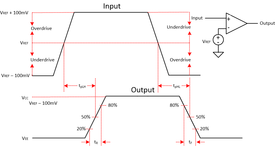
There is a delay between from when the input crosses the reference voltage and the output responds. This is called the Propagation Delay. Propagation delay can be different between high-to low and low-to-high input transitions. This is shown as tpLH and tpHL in Figure 9-1 and is measured from the mid-point of the input to the midpoint of the output.
GUID-7EEDC5D9-84C4-4C3F-89E4-C7F8B4569509-low.pngFigure 9-1 Comparator Timing Diagram