SBOS533B September 2010 – October 2015 TLV3501A-Q1
PRODUCTION DATA.
- 1 Features
- 2 Applications
- 3 Description
- 4 Revision History
- 5 Related Products
- 6 Pin Configuration and Functions
- 7 Specifications
- 8 Detailed Description
- 9 Application and Implementation
- 10Power Supply Recommendations
- 11Layout
- 12Device and Documentation Support
- 13Mechanical, Packaging, and Orderable Information
9 Application and Implementation
NOTE
Information in the following applications sections is not part of the TI component specification, and TI does not warrant its accuracy or completeness. TI’s customers are responsible for determining suitability of components for their purposes. Customers should validate and test their design implementation to confirm system functionality.
9.1 Application Information
9.1.1 Adding External Hysteresis
The TLV3501A-Q1 device has a robust performance when used with a good layout. However, the comparator inputs have little noise immunity within the range of specified offset voltage (±5 mV). For slow moving or noisy input signals, the comparator output can cause an undesirable switch state as input signals move through the switching threshold. In such applications, the 6 mV of internal hysteresis of the TLV3501A-Q1 device might not be sufficient. In cases where greater noise immunity is desired, external hysteresis can be added by connecting a small amount of feedback to the positive. Figure 17 shows a typical topology used to introduce 25 mV of additional hysteresis, for a total of 31-mV hysteresis when operating from a single 5-V supply. Use Equation 1 to calculate the approximate total hysteresis.

The total hysteresis, VHYST, sets the value of the transition voltage required to switch the comparator output by enlarging the threshold region, thereby reducing sensitivity to noise.
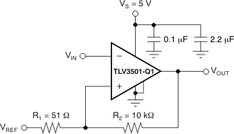 Figure 17. Adding Hysteresis to the TLV3501A-Q1
9.2 Typical Application
9.2.1 Relaxation Oscillator
The TLV3501A-Q1 device can easily be configured as a simple and inexpensive relaxation oscillator. In Figure 18, the R2 network sets the trip threshold at 1/3 and 2/3 of the supply. Because this circuit is a high-speed circuit, the resistor values are rather low to minimize the effect of parasitic capacitance. The positive input alternates between 1/3 of V+ and 2/3 of V+ depending on whether the output is low or high. The time to charge (or discharge) is 0.69 × R1C. Therefore, the period is 1.38 × R1C. For 62 pF and 1 kΩ as shown in Figure 18, the output is calculated to be 10.9 MHz. An implementation of this circuit oscillated at 9.6 MHz. Parasitic capacitance and component tolerances explain the difference between theory and actual performance.
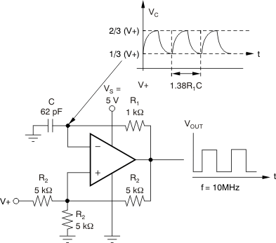 Figure 18. Relaxation Oscillator
9.2.1.1 Design Requirements
For hysteresis of 1/3 of V+ and threshold levels between 1/3 of V+ and 2/3 of V+, the resistors connected to comparator positive input should be equal in value. The resistor value should be kept low enough so it does not create additional time constant because of the input capacitor and board parasitic capacitor. The value of the charging resistor, R1, should be relatively low for high frequency switching without drawing high current and effecting the output high and low level. The value of the charging capacitor should be high enough to avoid errors cause by parasitic capacitance.
9.2.1.2 Detailed Design Procedure
For the positive input, +IN = 1/3 VOUT + 1/3 V+ = 1/3 V+ if VOUT is low and assuming VOL is very close to GND. Or, +IN = 1/3 VOUT + 1/3 V+ = 1/3 V+ = 2/3 V+ if VOUT is high and assuming VOH is very close to V+.
For the negative input, the capacitor charges to 2/3 V+ and discharges to 1/3 V+ exponentially at the same rate with a time constant of R1C.
9.2.1.3 Application Curve
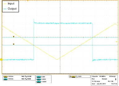 Figure 19. TLV3501A-Q1 Device With Upper and Lower Threshold With 1-V Hysteresis
9.2.2 High-Speed Window Comparator
A window comparator circuit is used to determine when a signal is between two voltages. The TLV3501A-Q1 device can readily be used to create a high-speed window comparator. The VHI value is the upper voltage threshold, and the VLO value is the lower voltage threshold. When VIN is between these two thresholds, the output in Figure 20 is high. Figure 21 shows a simple means of obtaining an active low output. Note that the reference levels are connected differently between Figure 20 and Figure 21. The operating voltage range of either circuit is 2.7 V to 5.5 V.
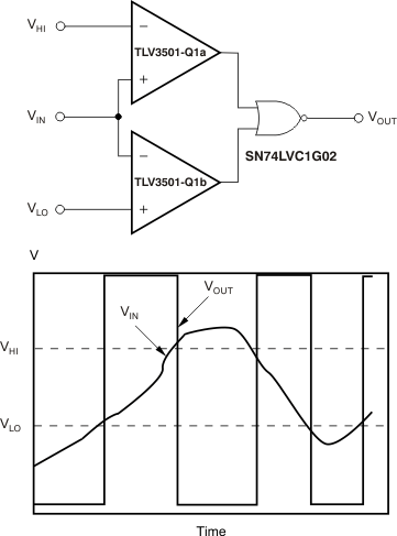 Figure 20. Window Comparator: Active High
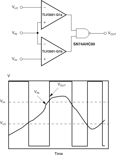 Figure 21. Window Comparator: Active Low