-
TLV354x 200MHz、レール・ツー・レールI/O、コスト制限の厳しいシステム向けのCMOSオペアンプ
- 1 特長
- 2 アプリケーション
- 3 概要
- 4 改訂履歴
- 5 Pin Configuration and Functions
- 6 Specifications
- 7 Detailed Description
- 8 Application and Implementation
- 9 Power Supply Recommendations
- 10Layout
- 11デバイスおよびドキュメントのサポート
- 12メカニカル、パッケージ、および注文情報
- 重要なお知らせ
TLV354x 200MHz、レール・ツー・レールI/O、コスト制限の厳しいシステム向けのCMOSオペアンプ
1 特長
- 低コストのシステム用の広帯域アンプ
- ユニティ・ゲイン帯域幅: 200MHz
- 高いスルー・レート: 150V/μs
- 低ノイズ: 7.5nV/√Hz
- レール・ツー・レールI/O
- 高い出力電流: 100mA超
- 非常に優れたビデオ性能
- 差動ゲイン: 0.02%、差動位相: 0.09°
- 0.1dBのゲイン・フラットネス(40MHz)
- 低い入力バイアス電流: 3pA
- 静止電流: 5.2mA
- サーマル・シャットダウン
- 電源電圧範囲: 2.5V~5.5V
2 アプリケーション
- 高分解能のADCドライバ・アンプ
- IRタッチ
- 低電圧、高周波数の信号処理
- ビデオ処理
- トランシーバ基地局
- 光ネットワーク、調節可能なレーザー
- フォトダイオード・トランスインピーダンス・アンプ
- バーコード・スキャナ
- 高速電流センス・アンプ
- 超音波イメージング
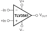 Figure 1. 概略回路図
3 概要
TLV3541、TLV3542、TLV3544はシングル、デュアル、クワッド・チャネルで低消費電力(チャネルごとに5.2mA)、高速、ユニティ・ゲイン安定、レール・ツー・レール入力/出力のオペアンプであり、広い帯域幅を必要とするビデオやその他のアプリケーション用に設計されています。
これらのデバイスは、電源からわずか6.5mA (最大値)の電流しか消費せず、200MHzのゲイン帯域幅積、150V/μsのスルー・レート、およびf = 1MHzにおいて7.5 nV/√Hzの低い入力ノイズを実現しています。高帯域幅、高いスルー・レート、低いノイズを併せ持つため、TLV354xファミリは低電圧、高速の信号コンディショニング・システムに適しています。
TLV354xシリーズのオペアンプは、最低2.5V (±1.25V)、最高5.5V (±2.75V)のシングルまたはデュアル電源で動作するよう最適化されています。同相入力範囲は電源の範囲よりも拡大されています。出力スイングはレールから100mV以内で、広いダイナミックレンジに対応しています。
TLV354xデバイスは、-40℃~+125℃での動作が規定されています。TLV354xファミリは、市販されている多くの広帯域オペアンプのプラグイン代替品として使用できます。
製品情報(1)
| 型番 | パッケージ | 本体サイズ(公称) |
|---|---|---|
| TLV3541 | SOIC (8) | 3.91mm×4.90mm |
| SOT-23 (5) | 2.90mm×1.60mm | |
| TLV3542 | SOIC (8) | 3.91mm×4.90mm |
| VSSOP (8) | 3.00mm×3.00mm | |
| TLV3544 | SOIC (14) | 8.65mm×3.91mm |
| TSSOP (14) | 5.00mm×4.40mm |
- 提供されているすべてのパッケージについては、巻末の注文情報を参照してください。
4 改訂履歴
| 日付 | 改訂内容 | 注 |
|---|---|---|
| 2016年10月 | * | 初版 |
5 Pin Configuration and Functions


Pin Functions: TLV3541
| PIN | I/O | DESCRIPTION | ||
|---|---|---|---|---|
| NAME | DBV (SOT-23) | D (SOIC) | ||
| –IN | 4 | 2 | I | Inverting input |
| +IN | 3 | 3 | I | Noninverting input |
| NC | — | 1, 5, 8 | — | No internal connection (can be left floating) |
| OUT | 1 | 6 | O | Output |
| V– | 2 | 4 | — | Negative (lowest) supply |
| V+ | 5 | 7 | — | Positive (highest) supply |

Pin Functions: TLV3542
| PIN | I/O | DESCRIPTION | |
|---|---|---|---|
| NAME | NO. | ||
| –IN A | 2 | I | Inverting input, channel A |
| +IN A | 3 | I | Noninverting input, channel A |
| –IN B | 6 | I | Inverting input, channel B |
| +IN B | 5 | I | Noninverting input, channel B |
| OUT A | 1 | O | Output, channel A |
| OUT B | 7 | O | Output, channel B |
| V– | 4 | — | Negative (lowest) supply |
| V+ | 8 | — | Positive (highest) supply |

Pin Functions: TLV3544
| PIN | I/O | DESCRIPTION | ||
|---|---|---|---|---|
| NAME | TLV3544 | |||
| D (SOIC) | PW (TSSOP) | |||
| –IN A | 2 | 2 | I | Inverting input, channel A |
| –IN B | 6 | 6 | I | Inverting input, channel B |
| –IN C | 9 | 9 | I | Inverting input, channel C |
| –IN D | 13 | 13 | I | Inverting input, channel D |
| +IN A | 3 | 3 | I | Noninverting input, channel A |
| +IN B | 5 | 5 | I | Noninverting input, channel B |
| +IN C | 10 | 10 | I | Noninverting input, channel C |
| +IN D | 12 | 12 | I | Noninverting input, channel D |
| OUT A | 1 | 1 | O | Output, channel A |
| OUT B | 7 | 7 | O | Output, channel B |
| OUT C | 8 | 8 | O | Output, channel C |
| OUT D | 14 | 14 | O | Output, channel D |
| V– | 11 | 11 | — | Negative (lowest) supply |
| V+ | 4 | 4 | — | Positive (highest) supply |
6 Specifications
6.1 Absolute Maximum Ratings
over operating free-air temperature range (unless otherwise noted)(1)| MIN | MAX | UNIT | ||
|---|---|---|---|---|
| Voltage | Supply voltage, V+ to V− | 7.5 | V | |
| Signal input terminals(2) | (V–) – (0.5) | (V+) + 0.5 | V | |
| Current | Signal input terminals(2) | –10 | 10 | mA |
| Output short circuit(3) | Continuous | |||
| Temperature | Operating, TA | –55 | 150 | °C |
| Junction, TJ | –65 | 150 | °C | |
| Storage, Tstg | 150 | °C | ||
6.2 ESD Ratings
| VALUE | UNIT | |||
|---|---|---|---|---|
| V(ESD) | Electrostatic discharge | Human-body model (HBM), per ANSI/ESDA/JEDEC JS-001(1) | 1000 | V |
| Charged-device model (CDM), per JEDEC specification JESD22-C101(2) | 250 | |||
6.3 Recommended Operating Conditions
over operating free-air temperature range (unless otherwise noted)| MIN | NOM | MAX | UNIT | ||
|---|---|---|---|---|---|
| VS | Supply voltage, V– to V+ | 2.5 | 5.5 | V | |
| Specified temperature range | –40 | 125 | °C | ||
6.4 Thermal Information: TLV3541
| THERMAL METRIC(1) | TLV3541 | UNIT | ||
|---|---|---|---|---|
| D (SOIC) | DBV (SOT-23) | |||
| 8 PINS | 5 PINS | |||
| RθJA | Junction-to-ambient thermal resistance | 123.8 | 216.3 | °C/W |
| RθJC(top) | Junction-to-case (top) thermal resistance | 68.7 | 84.3 | °C/W |
| RθJB | Junction-to-board thermal resistance | 64.5 | 43.1 | °C/W |
| ψJT | Junction-to-top characterization parameter | 23.0 | 3.8 | °C/W |
| ψJB | Junction-to-board characterization parameter | 64.0 | 42.3 | °C/W |
| RθJC(bot) | Junction-to-case (bottom) thermal resistance | N/A | N/A | °C/W |
6.5 Thermal Information: TLV3542
| THERMAL METRIC(1) | TLV3542 | UNIT | ||
|---|---|---|---|---|
| D (SOIC) | DGK (VSSOP) | |||
| 8 PINS | 8 PINS | |||
| RθJA | Junction-to-ambient thermal resistance | 113.9 | 175.9 | °C/W |
| RθJC(top) | Junction-to-case (top) thermal resistance | 60.4 | 67.8 | °C/W |
| RθJB | Junction-to-board thermal resistance | 54.1 | 97.1 | °C/W |
| ψJT | Junction-to-top characterization parameter | 17.1 | 9.3 | °C/W |
| ψJB | Junction-to-board characterization parameter | 53.6 | 95.5 | °C/W |
| RθJC(bot) | Junction-to-case (bottom) thermal resistance | N/A | N/A | °C/W |
6.6 Thermal Information: TLV3544
| THERMAL METRIC(1) | TLV3544 | UNIT | ||
|---|---|---|---|---|
| D (SOIC) | PW (TSSOP) | |||
| 14 PINS | 14 PINS | |||
| RθJA | Junction-to-ambient thermal resistance | 83.8 | 92.6 | °C/W |
| RθJC(top) | Junction-to-case (top) thermal resistance | 70.7 | 27.5 | °C/W |
| RθJB | Junction-to-board thermal resistance | 59.5 | 33.6 | °C/W |
| ψJT | Junction-to-top characterization parameter | 11.6 | 1.9 | °C/W |
| ψJB | Junction-to-board characterization parameter | 37.7 | 33.1 | °C/W |
| RθJC(bot) | Junction-to-case (bottom) thermal resistance | N/A | N/A | °C/W |
6.7 Electrical Characteristics: VS = 2.7 V to 5.5 V Single-Supply
at TA = 25°C, RF = 0 Ω, RL = 1 kΩ, and connected to VS / 2 (unless otherwise noted)| PARAMETER | TEST CONDITIONS | MIN | TYP | MAX | UNIT | ||
|---|---|---|---|---|---|---|---|
| OFFSET VOLTAGE | |||||||
| VOS | Input offset voltage | VS = 5 V, at TA = 25°C | ±2 | ±10 | mV | ||
| dVOS/dT | Input offset voltage vs temperature | VS = 5 V, at TA = −40°C to +125°C | ±4.5 | μV/°C | |||
| PSRR | Input offset voltage vs power supply | VS = 2.7 V to 5.5 V, VCM = (VS / 2) − 0.55 V |
60 | 70 | dB | ||
| INPUT BIAS CURRENT | |||||||
| IB | Input bias current | 3 | pA | ||||
| IOS | Input offset current | ±1 | pA | ||||
| NOISE | |||||||
| en | Input voltage noise density | f = 1 MHz | 7.5 | nV/√Hz | |||
| in | Current noise density | f = 1 MHz | 50 | fA/√Hz | |||
| INPUT VOLTAGE RANGE | |||||||
| VCM | Common-mode voltage range | (V−) − 0.1 | (V+) + 0.1 | V | |||
| CMRR | Common-mode rejection ratio | VS = 5.5 V, –0.1 V < VCM < 3.5 V, at TA = 25°C |
66 | 80 | dB | ||
| VS = 5.5 V, –0.1 V < VCM < 5.6 V, at TA = 25°C |
56 | 68 | dB | ||||
| INPUT IMPEDANCE | |||||||
| Differential | 1013 || 2 | Ω || pF | |||||
| Common-mode | 1013 || 2 | Ω || pF | |||||
| OPEN-LOOP GAIN | |||||||
| AOL | Open-loop gain | VS = 5 V, 0.3 V < VO < 4.7 V, at TA = 25°C |
92 | 108 | dB | ||
| FREQUENCY RESPONSE | |||||||
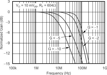
| f−3dB | Small-signal bandwidth | At G = +1, VO = 10 mV RF = 25 Ω |
200 | MHz | |||
| At G = +2, VO = 10 mV | 90 | MHz | |||||
| GBW | Gain-bandwidth product | G = +10 | 100 | MHz | |||
| f0.1dB | Bandwidth for 0.1-dB gain flatness | At G = +2, VO = 10 mV | 40 | MHz | |||
| SR | Slew rate | VS = 5 V, G = +1, 4-V step | 150 | V / μs | |||
| VS = 5 V, G = +1, 2-V step | 130 | V / μs | |||||
| Rise-and-fall time | At G = +1, VO = 200 mVPP, 10% to 90% |
2 | ns | ||||
| At G = +1, VO = 2 VPP, 10% to 90% | 11 | ns | |||||
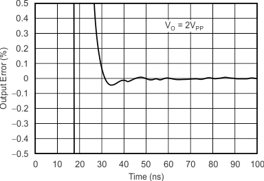
| Settling time | 0.1%, VS = 5 V, G = +1, 2-V output step |
30 | ns | ||||
| 0.01%, VS = 5 V, G = +1, 2-V output step |
60 | ns | |||||
| Overload recovery time | VIN × Gain = VS | 5 | ns | ||||
| FREQUENCY RESPONSE, continued | |||||||
| Harmonic distortion | Second harmonic | At G = +1, f = 1 MHz, VO = 2 VPP, RL = 200 Ω, VCM = 1.5 V |
–75 | dBc | |||
| Third harmonic | At G = +1, f = 1 MHz, VO = 2 VPP, RL = 200 Ω, VCM = 1.5 V |
–83 | dBc | ||||
| Differential gain error | NTSC, RL = 150 Ω | 0.02% | |||||
| Differential phase error | NTSC, RL = 150 Ω | 0.09 | ° | ||||
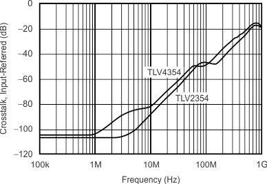
| Channel-to-channel crosstalk | TLV3542 | f = 5 MHz | –100 | dB | |||
| TLV3544 | –84 | dB | |||||
| OUTPUT | |||||||
| Voltage output swing from rail | VS = 5 V, RL = 1 kΩ at TA = 25°C | 0.1 | 0.3 | V | |||
| IO | Output current, single, dual, quad(1)(2) | VS = 5 V | 100 | mA | |||
| VS = 3 V | 50 | mA | |||||
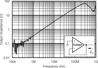
| Closed-loop output impedance | f < 100 kHz | 0.05 | Ω | ||||
| RO | Open-loop output resistance | 35 | Ω | ||||
| POWER SUPPLY | |||||||
| VS | Specified voltage range | 2.7 | 5.5 | V | |||
| Operating voltage range | 2.5 | 5.5 | V | ||||
| IQ | Quiescent current (per amplifier) | At TA = 25°C, VS = 5 V, IO = 0 |
5.2 | 6.5 | mA | ||
| TEMPERATURE RANGE | |||||||
| Specified range | –40 | 125 | °C | ||||
| Operating range (3) | –55 | 150 | °C | ||||
| Storage range | –65 | 150 | °C | ||||
| THERMAL SHUTDOWN | |||||||
| Shutdown temperature | 160 | °C | |||||
| Reset from shutdown | 140 | °C | |||||
6.8 Typical Characteristics
at TA = 25°C, VS = 5 V, G = +1, RF = 0 Ω, RL = 1 kΩ, and connected to VS / 2, unless otherwise noted.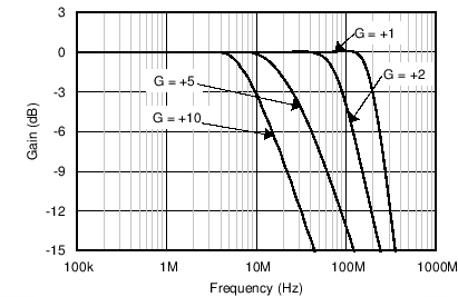
| RF = 604 Ω | VO = 10 mVpp |
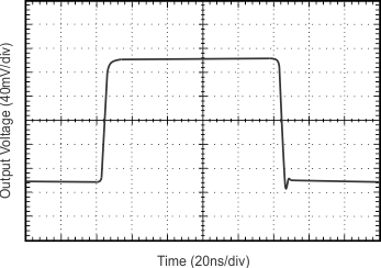
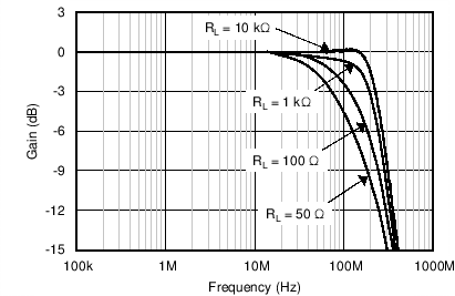
| G = +1, RF = 0 Ω | VO = 10 mVpp | CL = 0 pF |
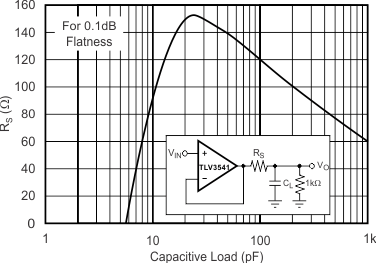
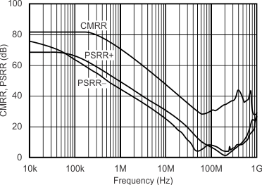
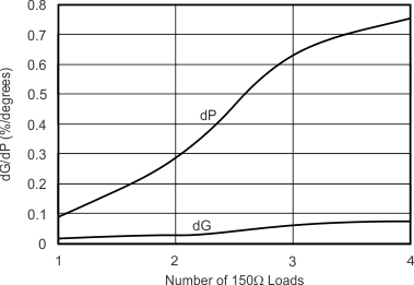
for VS = 3 V
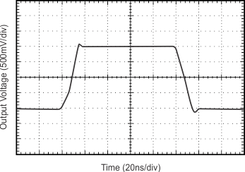
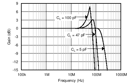
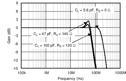
| G = +1, RS = 0 Ω | VO = 10 mVpp |
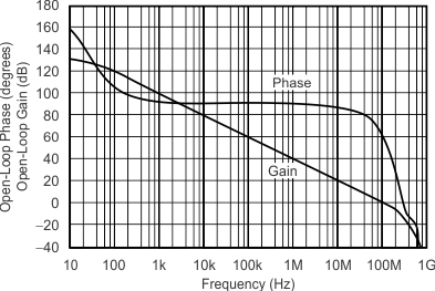
| G = +1, VO = 10 mVpp | ||
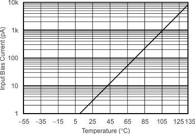
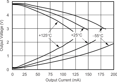
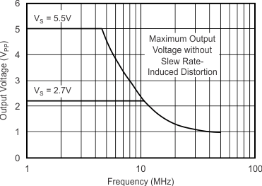
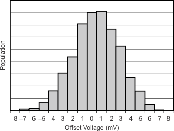
for VS = 5 V
7 Detailed Description
7.1 Overview
The TLV354x is a CMOS, rail-to-rail I/O, high-speed, voltage-feedback operational amplifier designed for video, high-speed, and other applications. The device is available as a single, dual, or quad op amp.
The amplifier features a 100-MHz gain bandwidth and a 150-V/μs slew rate, but the amplifier is unity-gain stable and operates as a +1-V/V voltage follower.
7.2 Functional Block Diagram

7.3 Feature Description
7.3.1 Operating Voltage
The TLV354x is specified over a power-supply range of 2.7 V to 5.5 V (±1.35 V to ±2.75 V). However, the supply voltage may range from 2.5 V to 5.5 V (±1.25 V to ±2.75 V). Supply voltages higher than 7.5 V (absolute maximum) can permanently damage the amplifier.
Parameters that vary over supply voltage or temperature are shown in the Typical Characteristics section.
7.3.2 Rail-to-Rail Input
The specified input common-mode voltage range of the TLV354x extends 100 mV beyond the supply rails. This extended range is achieved with a complementary input stage: an N-channel input differential pair in parallel with a P-channel differential pair, as shown in the Functional Block Diagram. The N-channel pair is active for input voltages close to the positive rail, typically (V+) − 1.2 V to 100 mV above the positive supply, while the P-channel pair is on for inputs from 100 mV below the negative supply to approximately (V+) − 1.2 V. There is a small transition region, typically (V+) − 1.5 V to (V+) − 0.9 V, in which both pairs are on. This 600-mV transition region can vary ±500 mV with process variation. Thus, the transition region ( with both input stages on) can range from (V+) − 2.0 V to (V+) − 1.5 V on the low end, up to (V+) − 0.9 V to (V+) − 0.4 V on the high end.
A double-folded cascode adds the signal from the two input pairs and presents a differential signal to the class AB output stage.
7.3.3 Rail-to-Rail Output
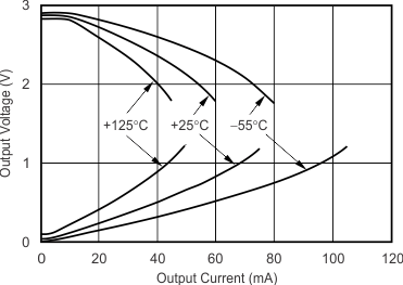
A class AB output stage with common-source transistors is used to achieve rail-to-rail output. For high-impedance loads (> 200 Ω), the output voltage swing is typically 100 mV from the supply rails. With 10-Ω loads, a useful output swing can be achieved while maintaining high open-loop gain. See the typical characteristic curves, Output Voltage Swing vs Output Current (Figure 14 and Figure 15).
7.3.4 Output Drive
The TLV354x output stage can supply a continuous output current of ±100 mA and yet provide approximately 2.7 V of output swing on a 5-V supply, as shown in Figure 21. For maximum reliability, it is not recommended to run a continuous DC current in excess of ±100 mA. Refer to the typical characteristic curves, Output Voltage Swing vs Output Current (Figure 14 and Figure 15). For supplying continuous output currents greater than ±100 mA, the TLV354x may be operated in parallel, as shown in Figure 22.
 Figure 21. Laser Diode Driver
The TLV354x provides peak currents up to 200 mA, which corresponds to the typical short-circuit current. Therefore, an on-chip thermal shutdown circuit is provided to protect the TLV354x from dangerously high junction temperatures. At 160°C, the protection circuit shuts down the amplifier. Normal operation resumes when the junction temperature cools to below +140°C.
 Figure 22. Parallel Operation
7.3.5 Video
The TLV354x output stage is capable of driving standard back-terminated 75-Ω video cables, as shown in Figure 23. By back-terminating a transmission line, the device does not exhibit a capacitive load to its driver. A properly back-terminated 75-Ω cable does not appear as capacitance; the device presents a 150-Ω resistive load to the TLV354x output.
 Figure 23. Single-Supply Video Line Driver
The TLV3542 can be used as an amplifier for RGB graphic signals, which have a voltage of zero at the video black level, by offsetting and AC-coupling the signal. See Figure 24.

7.3.6 Driving Analog-to-Digital Converters
The TLV354x series op amps offer 60 ns of settling time to 0.01%, making them a good choice for driving high- and medium-speed sampling A/D converters and buffering reference circuits. The TLV354x series provide an effective means of buffering the A/D converter input capacitance and resulting charge injection while providing signal gain. For applications requiring high DC accuracy, TI recommends using the OPA350 series.
Figure 25 illustrates the TLV3541 driving an A/D converter. With the TLV3541 in an inverting configuration, a capacitor across the feedback resistor can filter high-frequency noise in the signal.
 Figure 25. The TLV3541 in Inverting Configuration Driving the ADS7816
7.3.7 Capacitive Load and Stability
The TLV354x series op amps can drive a wide range of capacitive loads. However, all op amps under certain conditions may become unstable. Op amp configuration, gain, and load value are just a few of the factors to consider when determining stability. An op amp in unity-gain configuration is most susceptible to the effects of capacitive loading. The capacitive load reacts with the device output resistance, along with any additional load resistance, to create a pole in the small-signal response that degrades the phase margin. Refer to the typical characteristic curve, Frequency Response for Various CL (Figure 7) for details.
The TLV354x topology enhances the ability to drive capacitive loads. In unity gain, these op amps perform well with large capacitive loads. Refer to the typical characteristic curves, Recommended RS vs Capacitive Load (Figure 8) and Frequency Response vs Capacitive Load (Figure 9) for details.
One method of improving capacitive load drive in the unity-gain configuration is to insert a 10-Ω to 20-Ω resistor in series with the output, as shown in Figure 26. This configuration significantly reduces ringing with large capacitive loads. See the typical characteristic curve, Frequency Response vs Capacitive Load (Figure 9). However, if there is a resistive load in parallel with the capacitive load, RS creates a voltage divider. This voltage division introduces a DC error at the output and slightly reduces output swing. This error may be insignificant. For instance, with RL = 10 kΩ and RS = 20 Ω, there is an error of approximately 0.2% at the output.
 Figure 26. Series Resistor in Unity-Gain Configuration Improves Capacitive Load Drive
7.3.8 Wideband Transimpedance Amplifier
Wide bandwidth, low input bias current, and low input voltage and current noise make the TLV354x a suitable wideband photodiode transimpedance amplifier for low-voltage, single-supply applications. Low-voltage noise is important because photodiode capacitance causes the effective noise gain of the circuit to increase at high frequency.
The key elements to a transimpedance design, as shown in Figure 27, are the expected diode capacitance (including the parasitic input common-mode and differential-mode input capacitance (2 + 2) pF for the TLV354x), the desired transimpedance gain (RF), and the Gain-Bandwidth Product (GBW) for the TLV354x (100 MHz, typical). With these three variables set, the feedback capacitor value (CF) may be set to control the frequency response.
 Figure 27. Transimpedance Amplifier
To achieve a flat, second-order, Butterworth frequency response, the feedback pole must be set as shown in Equation 1:

Typical surface-mount resistors have a parasitic capacitance of approximately 0.2 pF that must be deducted from the calculated feedback capacitance value. Bandwidth is calculated by Equation 2:

For even higher transimpedance bandwidth, the high-speed CMOS OPA355 (200-MHz GBW) or the OPA655 (400-MHz GBW) may be used.
7.4 Device Functional Modes
The TLV354x has dual functional modes and is operational when the power-supply voltage is greater than 2.5 V (±1.25 V). The maximum power-supply voltage for the TLV354x is 5.5 V (±2.75 V). At +160°C, the protection circuit shuts down the amplifier. Normal operation resumes when the junction temperature cools to below +140°C.
8 Application and Implementation
NOTE
Information in the following applications sections is not part of the TI component specification, and TI does not warrant its accuracy or completeness. TI’s customers are responsible for determining suitability of components for their purposes. Customers should validate and test their design implementation to confirm system functionality.
8.1 Application Information
The TLV354x are wide bandwidth, low-noise, rail-to-rail input and output amplifiers. These devices operate from 2.5 V to 5.5 V, are unity-gain stable, and suitable for a wide range of general-purpose applications The input common-mode voltage range includes both rails, and allows the TLV354x device to be used in any single-supply application. Rail-to-rail input and output swing significantly increases dynamic range, especially in low-supply applications, and makes the device ideal for driving analog-to-digital converters (ADCs).
The TLV354x family of devices features a 200-MHz bandwidth and 150-V/μs slew rate with only 7.5 nV/√Hz of broadband noise.
8.2 Typical Application
A typical application for an operational amplifier is an inverting amplifier, as shown in Figure 28. An inverting amplifier takes a positive voltage on the input and outputs a signal inverted to the input, making a negative voltage of the same magnitude. In the same manner, the amplifier makes negative input voltages positive on the output. In addition, amplification can be added by selecting the input resistor RI and the feedback resistor RF.
 Figure 28. Application Schematic
8.2.1 Design Requirements
The supply voltage must be chosen to be larger than the input voltage range and the desired output range. The limits of the input common-mode range (VCM) and the output voltage swing to the rails (VO) must be considered. For instance, this application scales a signal of ±0.5 V (1 V) to ±1.8 V (3.6 V). Setting the supply at ±2.5 V is sufficient to accommodate this application.
8.2.2 Detailed Design Procedure
Determine the gain required by the inverting amplifier using Equation 3 and Equation 4:


When the desired gain is determined, select a value for RI or RF. Selecting a value in the kilo ohm range is desirable for general-purpose applications because the amplifier circuit uses currents in the milliamp range. This milliamp current range ensures the device does not draw too much current. The trade-off is that large resistors (100s of kilo ohms) draw the smallest current but generate the highest noise. Small resistors (100s of ohms) generate low noise but draw high current. This example uses 10 kΩ for RI, meaning 36 kΩ is used for RF. These values are determined by Equation 5:

8.2.3 Application Curve
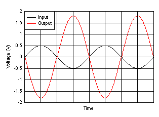 Figure 29. Inverting Amplifier Input and Output
8.3 System Examples
When receiving low-level signals, limiting the bandwidth of the incoming signals into the system is often required. The simplest way to establish this limited bandwidth is to place an RC filter at the noninverting terminal of the amplifier, as shown in Figure 30.
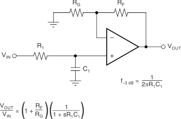 Figure 30. Single-Pole, Low-Pass Filter
If even more attenuation is needed, a multiple pole filter is required. The Sallen-Key filter can be used for this task, as shown in Figure 31. For best results, the amplifier must have a bandwidth that is eight to ten times the filter frequency bandwidth. Failure to follow this guideline can result in phase shift of the amplifier.
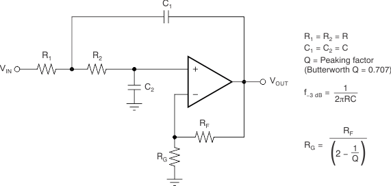 Figure 31. Two-Pole, Low-Pass, Sallen-Key Filter