JAJSNH8B December   2022  – September 2023 TLV2365 , TLV365

PRODUCTION DATA  

  1.   1
  2. 特長
  3. アプリケーション
  4. 概要
  5. Revision History
  6. Device Comparison Table
  7. Pin Configuration and Functions
  8. Specifications
    1. 7.1 Absolute Maximum Ratings
    2. 7.2 ESD Ratings
    3. 7.3 Recommended Operating Conditions
    4. 7.4 Thermal Information
    5. 7.5 Electrical Characteristics
    6. 7.6 Typical Characteristics
  9. Detailed Description
    1. 8.1 Overview
    2. 8.2 Functional Block Diagram
    3. 8.3 Feature Description
      1. 8.3.1 Rail-to-Rail Input
      2. 8.3.2 Input and ESD Protection
      3. 8.3.3 Driving Capacitive Loads
      4. 8.3.4 Active Filter
    4. 8.4 Device Functional Modes
  10. Application and Implementation
    1. 9.1 Application Information
      1. 9.1.1 Overdrive Recovery Performance
      2. 9.1.2 Achieving an Output Level of Zero Volts
    2. 9.2 Typical Applications
      1. 9.2.1 Second-Order Low-Pass Filter
        1. 9.2.1.1 Design Requirements
        2. 9.2.1.2 Detailed Design Procedure
        3. 9.2.1.3 Application Curve
      2. 9.2.2 ADC Driver and Reference Buffer
    3. 9.3 Power Supply Recommendations
    4. 9.4 Layout
      1. 9.4.1 Layout Guidelines
      2. 9.4.2 Layout Example
  11. 10Device and Documentation Support
    1. 10.1 Device Support
      1. 10.1.1 Development Support
        1. 10.1.1.1 PSpice® for TI
        2. 10.1.1.2 TINA-TI™シミュレーション・ソフトウェア (無償ダウンロード)
        3. 10.1.1.3 DIP アダプタ評価基板
        4. 10.1.1.4 DIYAMP-EVM
        5. 10.1.1.5 TI のリファレンス・デザイン
        6. 10.1.1.6 フィルタ設計ツール
    2. 10.2 Documentation Support
      1. 10.2.1 Related Documentation
    3. 10.3 ドキュメントの更新通知を受け取る方法
    4. 10.4 サポート・リソース
    5. 10.5 Trademarks
    6. 10.6 静電気放電に関する注意事項
    7. 10.7 用語集
  12. 11Mechanical, Packaging, and Orderable Information

パッケージ・オプション

メカニカル・データ(パッケージ|ピン)
サーマルパッド・メカニカル・データ
発注情報

Rail-to-Rail Input

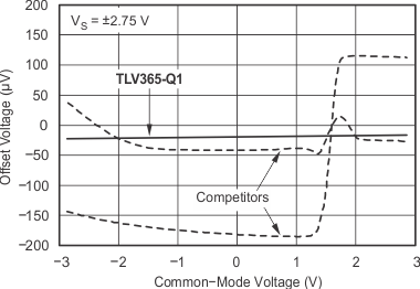
The TLVx365 product family features true rail-to-rail input operation, with supply voltages as low as ±1.1 V (2.2 V). A unique zerø-crossover input topology eliminates the input offset transition region typical of many rail-to-rail, complementary stage operational amplifiers. As shown in Figure 8-1, this topology also allows the TLVx365 to provide excellent common-mode performance over the entire input range, which extends 100 mV beyond both power-supply rails. When driving ADCs, the highly linear VCM range of the TLVx365 makes sure that the system linearity performance is not compromised. For a simplified schematic illustrating the rail-to-rail input circuitry, see Section 8.2.

GUID-9C4A13AF-86B7-4A95-BB0F-E6F938F135E9-low.gifFigure 8-1 TLVx365 Linear Offset Over the Entire Common-Mode Range