SBVS404A
April 2020 – June 2020
TLV4062
,
TLV4082
PRODUCTION DATA.
1
Features
2
Applications
3
Description
Device Images
Block Diagram for TLV4062
Block Diagram for TLV4082
4
Revision History
5
Pin Configuration and Functions
Pin Functions
6
Specifications
6.1
Absolute Maximum Ratings
6.2
ESD Ratings
6.3
Recommended Operating Conditions
6.4
Thermal Information
6.5
Electrical Characteristics
6.6
Timing Requirements
6.7
Typical Characteristics
7
Detailed Description
7.1
Overview
7.2
Functional Block Diagrams
7.3
Feature Description
7.4
Device Functional Modes
7.4.1
Inputs (IN1, IN2)
7.4.2
Outputs (OUT1, OUT2)
7.4.3
Switching Threshold and Hysteresis
8
Application and Implementation
8.1
Application Information
8.1.1
Threshold Overdrive
8.2
Typical Applications
8.2.1
Monitoring Two Separate Rails
8.2.1.1
Design Requirements
8.2.1.2
Detailed Design Procedure
8.2.1.3
Application Curve
8.2.2
Early Warning Detection
8.2.2.1
Design Requirements
8.2.2.2
Detailed Design Procedure
8.2.2.3
Application Curve
8.2.3
Additional Application Information
8.2.3.1
Pull-Up Resistor Selection
8.2.3.2
INx Capacitor
9
Power Supply Recommendations
10
Layout
10.1
Layout Guidelines
10.2
Layout Example
11
Device and Documentation Support
11.1
Documentation Support
11.1.1
Related Documentation
11.2
Receiving Notification of Documentation Updates
11.3
Related Links
11.4
Support Resources
11.5
Trademarks
11.6
Electrostatic Discharge Caution
11.7
Glossary
パッケージ・オプション
メカニカル・データ(パッケージ|ピン)
DRY|6
MPDS221F
DBV|6
MPDS026Q
サーマルパッド・メカニカル・データ
DRY|6
QFND138E
発注情報
sbvs404a_oa
sbvs404a_pm
6.6
Timing Requirements
typical values are at T
J
= 25°C and VDD = 3.3 V; INx transitions between 0 V and 1.3 V
MIN
NOM
MAX
UNIT
t
PD(r)
INx (rising) to OUTx propagation delay
5.5
µs
t
PD(f)
INx (falling) to OUTx propagation delay
10
µs
t
SD
Startup delay
(1)
570
µs
(1)
During power-on or when a VDD transient is below VDD(min), the outputs reflect the input conditions 570 µs after VDD transitions through VDD(min).
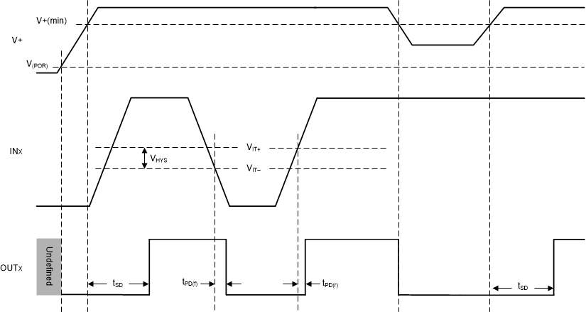
Figure 1.
Timing Diagram