JAJSD44B April   2017  – February 2021 TLV61046A

PRODUCTION DATA  

  1. 特長
  2. アプリケーション
  3. 概要
  4. Revision History
  5. Pin Configuration and Functions
  6. Specifications
    1. 6.1 Absolute Maximum Ratings
    2. 6.2 ESD Ratings
    3. 6.3 Recommended Operating Conditions
    4. 6.4 Thermal Information
    5. 6.5 Electrical Characteristics
    6. 6.6 Typical Characteristics
  7. Detailed Description
    1. 7.1 Overview
    2. 7.2 Functional Block Diagram
    3. 7.3 Feature Description
      1. 7.3.1 Undervoltage Lockout
      2. 7.3.2 Enable and Disable
      3. 7.3.3 Soft Start
      4. 7.3.4 Overvoltage Protection
      5. 7.3.5 Output Short Circuit Protection
      6. 7.3.6 Thermal Shutdown
    4. 7.4 Device Functional Modes
      1. 7.4.1 PWM Mode
      2. 7.4.2 Power Save Mode
  8. Application and Implementation
    1. 8.1 Application Information
    2. 8.2 Typical Application - 12-V Output Boost Converter
      1. 8.2.1 Design Requirements
      2. 8.2.2 Detailed Design Procedure
        1. 8.2.2.1 Custom Design With WEBENCH Tools
        2. 8.2.2.2 Programming the Output Voltage
        3. 8.2.2.3 Inductor Selection
        4. 8.2.2.4 Input and Output Capacitor Selection
      3. 8.2.3 Application Performance Curves
    3. 8.3 System Examples
      1. 8.3.1 Fixed 12-V Output Voltage with Three External Components
  9. Power Supply Recommendations
  10. 10Layout
    1. 10.1 Layout Guidelines
    2. 10.2 Layout Example
  11. 11Device and Documentation Support
    1. 11.1 Device Support
      1. 11.1.1 Third-Party Products Disclaimer
      2. 11.1.2 Development Support
        1. 11.1.2.1 Custom Design With WEBENCH® Tools
    2. 11.2 ドキュメントの更新通知を受け取る方法
    3. 11.3 サポート・リソース
    4. 11.4 Trademarks
    5. 11.5 静電気放電に関する注意事項
    6. 11.6 用語集
  12. 12Mechanical, Packaging, and Orderable Information

パッケージ・オプション

メカニカル・データ(パッケージ|ピン)
サーマルパッド・メカニカル・データ
発注情報

Programming the Output Voltage

There are two ways to set the output voltage of the TLV61046A. When the FB pin is connected to the input voltage, the output voltage is fixed to 12 V. This function makes the TLV61046A only need three external components to minimize the solution size. The second way is to use an external resistor divider to set the desired output voltage.

By selecting the external resistor divider R1 and R2, as shown in Equation 1, the output voltage is programmed to the desired value. When the output voltage is regulated, the typical voltage at the FB pin is VREF of 795 mV.
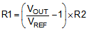
Equation 1. GUID-3D5D1701-7727-4C05-B4FD-A06BD709321B-low.gif

where

  • VOUT is the desired output voltage
  • VREF is the internal reference voltage at the FB pin

For best accuracy, R2 should be kept smaller than 80 kΩ to ensure the current flowing through R2 is at least 100 times larger than the FB pin leakage current. Changing R2 towards a lower value increases the immunity against noise injection. Changing the R2 towards a higher value reduces the quiescent current for achieving higher efficiency at low load currents.