JAJSH32 March   2019 TLV61048

ADVANCE INFORMATION for pre-production products; subject to change without notice.  

  1. 特長
  2. アプリケーション
  3. 概要
    1.     Device Images
      1.      概略回路図
  4. 改訂履歴
  5. Pin Configuration and Functions
    1.     Pin Functions
  6. Specifications
    1. 6.1 Absolute Maximum Ratings
    2. 6.2 ESD Ratings
    3. 6.3 Recommended Operating Conditions
    4. 6.4 Thermal Information
    5. 6.5 Electrical Characteristics
  7. Detailed Description
    1. 7.1 Overview
    2. 7.2 Functional Block Diagram
    3. 7.3 Feature Description
      1. 7.3.1 Undervoltage Lockout
      2. 7.3.2 Enable and Disable
      3. 7.3.3 Soft Start
      4. 7.3.4 Frequency Select (FREQ)
    4. 7.4 Device Functional Modes
      1. 7.4.1 PWM Mode
      2. 7.4.2 PFM Mode
  8. Application and Implementation
    1. 8.1 Application Information
    2. 8.2 Typical Applications
      1. 8.2.1 12-V Output Boost Converter With External Bias
        1. 8.2.1.1 Design Requirements
        2. 8.2.1.2 Detailed Design Procedure
          1. 8.2.1.2.1 Programming the Output Voltage
          2. 8.2.1.2.2 Inductor Selection
          3. 8.2.1.2.3 Input and Output Capacitor Selection
        3. 8.2.1.3 Application Curves
      2. 8.2.2 15-V Output Boost Converter
        1. 8.2.2.1 Design Requirements
        2. 8.2.2.2 Detailed Design Procedure
          1. 8.2.2.2.1 Inductor Selection
          2. 8.2.2.2.2 Input and Output Capacitor Selection
  9. Power Supply Recommendations
  10. 10Layout
    1. 10.1 Layout Guidelines
    2. 10.2 Layout Example
  11. 11デバイスおよびドキュメントのサポート
    1. 11.1 デバイス・サポート
      1. 11.1.1 デベロッパー・ネットワークの製品に関する免責事項
    2. 11.2 ドキュメントの更新通知を受け取る方法
    3. 11.3 コミュニティ・リソース
    4. 11.4 商標
    5. 11.5 静電気放電に関する注意事項
    6. 11.6 Glossary
  12. 12メカニカル、パッケージ、および注文情報

パッケージ・オプション

メカニカル・データ(パッケージ|ピン)
サーマルパッド・メカニカル・データ
発注情報

Pin Configuration and Functions

DBV Package
6-Pin SOT-23
Top View
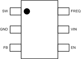
TLV61048 pinout_SLVSEX0.gif

Pin Functions

PIN I/O DESCRIPTION
NO. NAME
1 SW PWR The switch pin of the converter. It is connected to the drain of the internal power MOSFET.
2 GND PWR Ground
3 FB I Voltage feedback of adjustable output voltage. Connected to the center tap of a resistor divider to program the output voltage.
4 EN I Enable logic input. Logic high voltage enables the device. Logic low voltage disables the device and turns it into shutdown mode.
5 VIN I IC power supply input
6 FREQ I Frequency select pin. The device operates at 600 kHz if FREQ is left floating and at 1 MHz if connected to GND.