JAJSIJ5A
December 2020 – January 2023
TLV62595
PRODUCTION DATA
1
特長
2
アプリケーション
3
説明
4
Revision History
5
Pin Configuration and Functions
6
Specifications
6.1
Absolute Maximum Ratings
6.2
ESD Ratings
6.3
Recommended Operating Conditions
6.4
Thermal Information
6.5
電気的特性
6.6
Typical Characteristics
7
Detailed Description
7.1
Overview
7.2
Functional Block Diagram
7.3
Feature Description
7.3.1
Pulse Width Modulation (PWM) Operation
7.3.2
Power Save Mode (PSM) Operation
7.3.3
Minimum Duty Cycle and 100% Mode Operation
7.3.4
Soft Start
7.3.5
Switch Current Limit and HICCUP Short-Circuit Protection
7.3.6
Undervoltage Lockout
7.3.7
Thermal Shutdown
7.4
Device Functional Modes
7.4.1
Enable, Disable and Output Discharge
7.4.2
Power Good
8
Application and Implementation
8.1
Application Information
8.2
Typical Application
8.2.1
Design Requirements
8.2.2
Detailed Design Procedure
8.2.2.1
Custom Design With WEBENCH® Tools
8.2.2.2
Setting The Output Voltage
8.2.2.3
Output Filter Design
8.2.2.4
Inductor Selection
8.2.2.5
Capacitor Selection
8.2.3
Application Curves
8.3
Power Supply Recommendations
8.4
Layout
8.4.1
Layout Guidelines
8.4.2
Layout Example
8.4.2.1
Thermal Considerations
9
Device and Documentation Support
9.1
Device Support
9.1.1
サード・パーティ製品に関する免責事項
9.1.2
Development Support
9.1.2.1
Custom Design With WEBENCH® Tools
9.2
Documentation Support
9.2.1
Related Documentation
9.3
ドキュメントの更新通知を受け取る方法
9.4
サポート・リソース
9.5
Trademarks
9.6
静電気放電に関する注意事項
9.7
用語集
10
Mechanical, Packaging, and Orderable Information
パッケージ・オプション
メカニカル・データ(パッケージ|ピン)
DMQ|6
MPSS077D
サーマルパッド・メカニカル・データ
発注情報
jajsij5a_oa
jajsij5a_pm
8.2
Typical Application
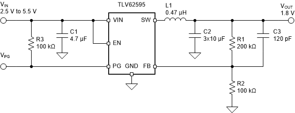
Figure 8-1
Typical Application of TLV62595