JAJSI98B
June 2016 – March 2021
TLV627432
PRODUCTION DATA
1
特長
2
アプリケーション
3
概要
4
Revision History
5
Device Comparison Table
6
Pin Configuration and Functions
7
Specifications
7.1
Absolute Maximum Ratings
7.2
ESD Ratings
7.3
Recommended Operating Conditions
7.4
Thermal Information
7.5
Electrical Characteristics
7.6
Timing Requirements
7.7
Typical Characteristics
8
Detailed Description
8.1
Overview
8.2
Functional Block Diagram
8.3
Feature Description
8.3.1
DCS-Control™
8.3.2
Power Save Mode Operation
8.3.3
Output Voltage Selection
8.3.4
Output Voltage Discharge of the Buck Converter
8.3.5
Undervoltage Lockout UVLO
8.3.6
Short circuit protection
8.4
Device Functional Modes
8.4.1
Enable and Shutdown
8.4.2
Device Start-up and Softstart
8.4.3
Automatic Transition Into No Ripple 100% Mode
9
Application and Implementation
9.1
Application Information
9.2
Typical Application
9.2.1
Design Requirements
9.2.2
Detailed Design Procedure
9.2.2.1
Inductor Selection
9.2.2.2
Output Capacitor Selection
9.2.2.3
Input Capacitor Selection
9.2.3
Application Curves
10
Power Supply Recommendations
11
Layout
11.1
Layout Guidelines
11.2
Layout Example
12
Device and Documentation Support
12.1
Device Support
12.1.1
Third-Party Products Disclaimer
12.2
Receiving Notification of Documentation Updates
12.3
サポート・リソース
12.4
Trademarks
12.5
静電気放電に関する注意事項
12.6
用語集
13
Mechanical, Packaging, and Orderable Information
パッケージ・オプション
メカニカル・データ(パッケージ|ピン)
YFP|8
MXBG057R
サーマルパッド・メカニカル・データ
発注情報
jajsi98b_oa
jajsi98b_pm
7.7
Typical Characteristics
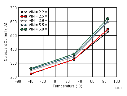
EN = VIN, V
OUT
= 1.8V
Device Not Switching
Figure 7-1
Quiescent Current vs Temperature
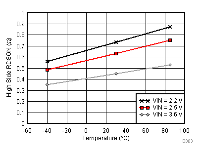
Figure 7-3
High Side R
DSON
vs Temperature
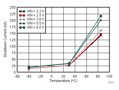
EN = GND
Figure 7-2
Shutdown Current I
SD
vs Temperature
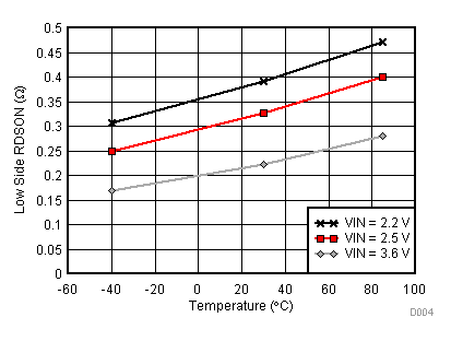
Figure 7-4
Low-side R
DSON
vs Temperature