JAJS514D September 2010 – July 2019 TLV702
PRODUCTION DATA.
- 1 特長
- 2 アプリケーション
- 3 概要
- 4 改訂履歴
- 5 Pin Configuration and Functions
- 6 Specifications
- 7 Detailed Description
- 8 Application and Implementation
- 9 Power Supply Recommendations
- 10Layout
- 11デバイスおよびドキュメントのサポート
- 12メカニカル、パッケージ、および注文情報
パッケージ・オプション
メカニカル・データ(パッケージ|ピン)
サーマルパッド・メカニカル・データ
発注情報
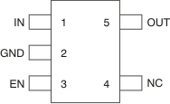
5 Pin Configuration and Functions
DSE Package
6-Pin WSON
Top View

Pin Functions
| PIN | I/O | DESCRIPTION | ||
|---|---|---|---|---|
| NAME | SOT-23 | WSON | ||
| IN | 1 | 1 | I | Input pin. A small, 1-μF ceramic capacitor is recommended from this pin to ground to assure stability and good transient performance. See in Application Information for more details. |
| GND | 2 | 2 | — | Ground pin |
| EN | 3 | 6 | I | Enable pin. Driving EN over 0.9 V turns on the regulator. Driving EN below 0.4 V puts the regulator into shutdown mode and reduces operating current to 1 μA, nominal.
For TLV702P, output voltage is discharged through an internal 120-Ω resistor when device is shut down. |
| NC | 4 | 4, 5 | — | No connection. This pin can be tied to ground to improve thermal dissipation. |
| OUT | 5 | 3 | O | Regulated output voltage pin. A small, 1-μF ceramic capacitor is needed from this pin to ground to assure stability. See in Application Information for more details. |
