JAJSUX8 June   2024 TLV9104-Q1

PRODMIX  

  1.   1
  2. 特長
  3. アプリケーション
  4. 概要
  5. Pin Configuration and Functions
  6. Specifications
    1. 5.1 Absolute Maximum Ratings
    2. 5.2 ESD Ratings
    3. 5.3 Recommended Operating Conditions
    4. 5.4 Thermal Information for Quad Channel
    5. 5.5 Electrical Characteristics
    6. 5.6 Typical Characteristics
  7. Detailed Description
    1. 6.1 Overview
    2. 6.2 Functional Block Diagram
    3. 6.3 Feature Description
      1. 6.3.1 EMI Rejection
      2. 6.3.2 Phase Reversal Protection
      3. 6.3.3 Thermal Protection
      4. 6.3.4 Capacitive Load and Stability
      5. 6.3.5 Common-Mode Voltage Range
      6. 6.3.6 Electrical Overstress
      7. 6.3.7 Overload Recovery
      8. 6.3.8 Typical Specifications and Distributions
    4. 6.4 Device Functional Modes
  8. Application and Implementation
    1. 7.1 Application Information
    2. 7.2 Typical Applications
      1. 7.2.1 Low-Side Current Measurement
        1. 7.2.1.1 Design Requirements
        2. 7.2.1.2 Detailed Design Procedure
        3. 7.2.1.3 Application Curve
    3. 7.3 Power Supply Recommendations
    4. 7.4 Layout
      1. 7.4.1 Layout Guidelines
      2. 7.4.2 Layout Example
  9. Device and Documentation Support
    1. 8.1 Device Support
      1. 8.1.1 Development Support
        1. 8.1.1.1 TINA-TI (Free Software Download)
    2. 8.2 Documentation Support
      1. 8.2.1 Related Documentation
    3. 8.3 ドキュメントの更新通知を受け取る方法
    4. 8.4 サポート・リソース
    5. 8.5 Trademarks
    6. 8.6 静電気放電に関する注意事項
    7. 8.7 用語集
  10. Revision History
  11. 10Mechanical, Packaging, and Orderable Information

パッケージ・オプション

メカニカル・データ(パッケージ|ピン)
サーマルパッド・メカニカル・データ
発注情報

Common-Mode Voltage Range

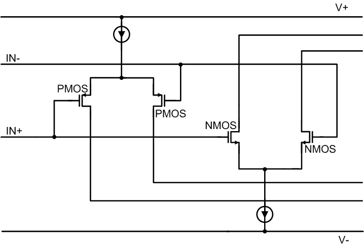
The TLV910x-Q1 is a 16V, true rail-to-rail input operational amplifier with an input common-mode range that extends 100mV beyond either supply rail. This wide range is achieved with paralleled complementary N-channel and P-channel differential input pairs, as shown in Figure 6-7. The N-channel pair is active for input voltages close to the positive rail, typically (V+) – 1V to 100mV above the positive supply. The P-channel pair is active for inputs from 100mV below the negative supply to approximately (V+) – 2V. There is a small transition region, typically (V+) –2V to (V+) – 1V in which both input pairs are on. This transition region can vary modestly with process variation, and within this region PSRR, CMRR, offset voltage, offset drift, noise, and THD performance can be degraded compared to operation outside this region. To achieve best performance with the TLV910x-Q1 family, avoid this transition region when possible.
TLV9104-Q1 Rail-to-Rail Input StageFigure 6-7 Rail-to-Rail Input Stage