JAJSJ16G May 2020 – March 2024 TLV9151-Q1 , TLV9152-Q1 , TLV9154-Q1
PRODUCTION DATA
- 1
- 1 特長
- 2 アプリケーション
- 3 概要
- 4 Pin Configuration and Functions
- 5 Specifications
- 6 Detailed Description
- 7 Application and Implementation
- 8 Device and Documentation Support
- 9 Revision History
- 10Mechanical, Packaging, and Orderable Information
パッケージ・オプション
メカニカル・データ(パッケージ|ピン)
サーマルパッド・メカニカル・データ
発注情報
6.3.4 Common-Mode Voltage Range
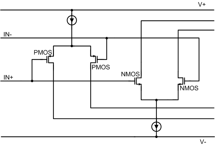
The TLV915x-Q1 is a 16-V, rail-to-rail input operational amplifier with an input common-mode range that extends 200 mV beyond either supply rail. This wide range is achieved with paralleled complementary N-channel and P-channel differential input pairs, as shown in Figure 6-6. The N-channel pair is active for input voltages close to the positive rail, typically (V+) – 1 V to 100 mV above the positive supply. The P-channel pair is active for inputs from 100 mV below the negative supply to approximately (V+) – 2 V. There is a small transition region, typically (V+) – 2 V to (V+) – 1 V in which both input pairs are on. This transition region can vary modestly with process variation, and within this region PSRR, CMRR, offset voltage, offset drift, noise, and THD performance may be degraded compared to operation outside this region.
Figure 5-5 shows this transition region for a typical device in terms of input voltage offset in more detail.
For more information on common-mode voltage range and PMOS/NMOS pair interaction, see Op Amps With Complementary-Pair Input Stages application note.
 Figure 6-6 Rail-to-Rail Input Stage