JAJSJ16G May 2020 – March 2024 TLV9151-Q1 , TLV9152-Q1 , TLV9154-Q1
PRODUCTION DATA
- 1
- 1 特長
- 2 アプリケーション
- 3 概要
- 4 Pin Configuration and Functions
- 5 Specifications
- 6 Detailed Description
- 7 Application and Implementation
- 8 Device and Documentation Support
- 9 Revision History
- 10Mechanical, Packaging, and Orderable Information
パッケージ・オプション
メカニカル・データ(パッケージ|ピン)
サーマルパッド・メカニカル・データ
発注情報
6.3.2 Thermal Protection
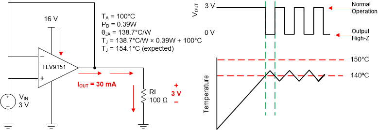
The internal power dissipation of any amplifier causes its internal (junction) temperature to rise. This phenomenon is called self heating. The absolute maximum junction temperature of the TLV915x-Q1 is 150°C. Exceeding this temperature causes damage to the device. The TLV915x-Q1 has a thermal protection feature that reduces damage from self heating. The protection works by monitoring the temperature of the device and turning off the op amp output drive for temperatures above 170°C. Figure 6-2 shows an application example for the TLV9151-Q1 that has significant self heating because of its power dissipation (0.81 W). Thermal calculations indicate that for an ambient temperature of 65°C, the device junction temperature will reach 177°C. The actual device, however, turns off the output drive to recover towards a safe junction temperature. Figure 6-2 shows how the circuit behaves during thermal protection. During normal operation, the device acts as a buffer so the output is 3 V. When self heating causes the device junction temperature to increase above the internal limit, the thermal protection forces the output to a high-impedance state and the output is pulled to ground through resistor RL. If the condition that caused excessive power dissipation is not removed, the amplifier will oscillate between a shutdown and enabled state until the output fault is corrected.
 Figure 6-2 Thermal Protection