JAJSTS7B March   2024  – August 2024 TMAG5213

PRODUCTION DATA  

  1.   1
  2. 特長
  3. アプリケーション
  4. 概要
  5. Device Comparison
  6. Pin Configuration and Functions
  7. Specifications
    1. 6.1 Absolute Maximum Ratings
    2. 6.2 ESD Ratings
    3. 6.3 Recommended Operating Conditions
    4. 6.4 Thermal Information
    5. 6.5 Electrical Characteristics
    6. 6.6 Switching Characteristics
    7. 6.7 Magnetic Characteristics
    8. 6.8 Typical Characteristics
  8. Detailed Description
    1. 7.1 Overview
    2. 7.2 Functional Block Diagram
    3. 7.3 Feature Description
      1. 7.3.1 Field Direction Definition
      2. 7.3.2 Device Output
      3. 7.3.3 Power-On Time
      4. 7.3.4 Output Stage
      5. 7.3.5 Protection Circuits
        1. 7.3.5.1 Overcurrent Protection (OCP)
    4. 7.4 Device Functional Modes
  9. Application and Implementation
    1. 8.1 Application Information
    2. 8.2 Typical Applications
      1. 8.2.1 Standard Circuit
        1. 8.2.1.1 Design Requirements
        2. 8.2.1.2 Detailed Design Procedure
          1. 8.2.1.2.1 Configuration Example
        3. 8.2.1.3 Application Curves
    3. 8.3 Power Supply Recommendations
    4. 8.4 Layout
      1. 8.4.1 Layout Guidelines
      2. 8.4.2 Layout Example
  10. Device and Documentation Support
    1. 9.1 Device Support
      1. 9.1.1 Device Nomenclature
      2. 9.1.2 Device Markings
    2. 9.2 ドキュメントの更新通知を受け取る方法
    3. 9.3 サポート・リソース
    4. 9.4 Trademarks
    5. 9.5 静電気放電に関する注意事項
    6. 9.6 用語集
  11. 10Revision History
  12. 11Mechanical, Packaging, and Orderable Information

パッケージ・オプション

メカニカル・データ(パッケージ|ピン)
サーマルパッド・メカニカル・データ
発注情報

Output Stage

Figure 7-8 shows the TMAG5213 open-drain NMOS output structure, rated to sink up to 30mA of current. For proper operation, use Equation 1 to calculate the value of pullup resistor R1.

Equation 1. V r e f   m a x 30 m A R 1 V r e f   m i n 100 μ A

The size of R1 is a tradeoff between the OUT rise time and the current when OUT is pulled low. A lower current is generally better, however faster transitions and bandwidth require a smaller resistor for faster switching.

In addition, make sure that the value of R1 > 500Ω so that the output driver can pull the OUT pin close to GND. Generally, TI recommends to use a resistor with a 10kΩ nominal value.

Note:

Vref is not restricted to VCC. The allowable voltage range of this pin is specified in the Absolute Maximum Ratings.
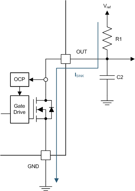
TMAG5213 NMOS Open-Drain Output Figure 7-8 NMOS Open-Drain Output

Select a value for C2 based on the system bandwidth specifications as shown in Equation 2.

Equation 2. 2 × f B W   H z < 1 2 π × R 1 × C 2

Most applications do not require this C2 filtering capacitor.