JAJSGC5D February 2011 – December 2018 TMP103
PRODUCTION DATA.
- 1 特長
- 2 アプリケーション
- 3 概要
- 4 改訂履歴
- 5 Pin Configuration and Functions
- 6 Specifications
-
7 Detailed Description
- 7.1 Overview
- 7.2 Functional Block Diagram
- 7.3 Feature Description
- 7.4 Device Functional Modes
- 7.5
Programming
- 7.5.1 Temperature Watchdog Function
- 7.5.2 Conversion Rate
- 7.5.3 Shutdown Mode (M1 = 0, M0 = 0)
- 7.5.4 One-Shot (M1 = 0, M0 = 1)
- 7.5.5 Continuous Conversion Mode (M1 = 1)
- 7.5.6 Bus Overview
- 7.5.7 Serial Interface
- 7.5.8 Serial Bus Address
- 7.5.9 Writing and Reading Operation
- 7.5.10 Slave Mode Operations
- 7.5.11 General Call
- 7.5.12 High-Speed (Hs) Mode
- 7.5.13 Timeout Function
- 7.5.14 Multiple Device Access
- 7.5.15 NOISE
- 7.6 Register Maps
- 8 Application and Implementation
- 9 Power Supply Recommendations
- 10Layout
- 11デバイスおよびドキュメントのサポート
- 12メカニカル、パッケージ、および注文情報
パッケージ・オプション
デバイスごとのパッケージ図は、PDF版データシートをご参照ください。
メカニカル・データ(パッケージ|ピン)
- YFF|4
サーマルパッド・メカニカル・データ
発注情報
7.5.2 Conversion Rate
The conversion rate bits, CR1 and CR0 located in the Configuration Register, configure the TMP103 for conversion rates of 8 Hz, 4 Hz, 1 Hz, or 0.25 Hz (default). The TMP103 has a typical conversion time of 26 ms. To achieve different conversion rates, the TMP103 performs a single conversion and then powers down and waits for the appropriate delay set by CR1 and CR0. Table 1 lists the settings for CR1 and CR0.
Table 1. Conversion Rate Settings
| CR1 | CR0 | CONVERSION RATE |
|---|---|---|
| 0 | 0 | 0.25 Hz (default) |
| 0 | 1 | 1 Hz |
| 1 | 0 | 4 Hz |
| 1 | 1 | 8 Hz |
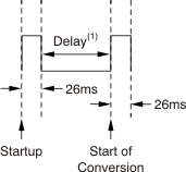
After power up or general-call reset, the TMP103 immediately starts a conversion, as shown in Figure 13. The first result is available after 26 ms (typical). The active quiescent current during conversion is 40 μA (typical at 27°C, V+ = 1.8 V). The quiescent current during delay is 1 μA (typical at 27°C, V+ = 1.8 V).
