SBOS759 November 2015 TMP175-Q1 , TMP75-Q1
PRODUCTION DATA.
- 1 Features
- 2 Applications
- 3 Description
- 4 Revision History
- 5 Pin Configuration and Functions
- 6 Specifications
- 7 Detailed Description
- 8 Application and Implementation
- 9 Power Supply Recommendations
- 10Layout
- 11Device and Documentation Support
- 12Mechanical, Packaging, and Orderable Information
1 Features
- AEC-Q100 Qualified with:
- Temperature Grade 1: –40°C to +125°C Ambient Operation Temperature Range
- HBM ESD Classification Level 2
- CDM ESD Classification Level C6
- TMP175-Q1 Accuracy:
- ±1°C (Typical) from –40°C to +125°C
- ±2°C (Maximum) from –40°C to +125°C
- TMP75-Q1 Accuracy:
- ±1°C (Typical) from –40°C to +125°C
- ±3°C (Maximum) from –40°C to +125°C
- TMP175-Q1: 27 Addresses
- TMP75-Q1: 8 Addresses, NIST Traceable
- Digital Output: SMBus™, Two-Wire, and I2C Interface Compatibility
- Resolution: 9 to 12 Bits, User-Selectable
- Low Quiescent Current: 50-μA, 0.1-μA Standby
- Wide Supply Range: 2.7 V to 5.5 V
- Small 8-Pin VSSOP and 8-Pin SOIC Packages
2 Applications
- Climate Controls
- Infotainment Processor Management
- Airflow Sensors
- Battery Control Units
- Engine Control Units
- UREA Sensors
- Water Pumps
- HID Lamps
- Airbag Control Units
Simplified Schematic

3 Description
The TMP75-Q1 and TMP175-Q1 devices are digital temperature sensors ideal for negative temperature coefficient (NTC) and positive temperature coefficient (PTC) thermistor replacement. The devices offer a typical accuracy of ±1°C without requiring calibration or external component signal conditioning. Device temperature sensors are highly linear and do not require complex calculations or look-up tables to derive the temperature. The on-chip, 12-bit, analog-to-digital converter (ADC) offers resolutions down to 0.0625°C. The devices are available in the industry-standard, LM75, 8-pin SOIC and VSSOP footprint.
The TMP175-Q1 and TMP75-Q1 feature SMBus, two-wire, and I2C interface compatibility. The TMP175-Q1 device allows up to 27 devices on one bus. The TMP75-Q1 allows up to eight devices on one bus. The TMP175-Q1 and TMP75-Q1 both feature an SMBus alert function.
The TMP175-Q1 and TMP75-Q1 devices are ideal for extended temperature measurement in a variety of communication, computer, consumer, environmental, industrial, and instrumentation applications. The TMP75-Q1 production units are 100% tested against sensors that are NIST-traceable and are verified with equipment that are NIST-traceable through ISO/IEC 17025 accredited calibrations.
The TMP175-Q1 and TMP75-Q1 devices are specified for operation over the temperature range of –40°C to +125°C.
Device Information(1)
| PART NUMBER | PACKAGE | BODY SIZE (NOM) |
|---|---|---|
| TMPx75-Q1 | SOIC (8) | 4.90 mm × 3.91 mm |
| VSSOP (8) | 3.00 mm × 3.00 mm |
- For all available packages, see the orderable addendum at the end of the data sheet.
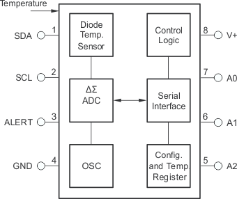
TMP175-Q1 and TMP75-Q1 Internal Block Diagram

4 Revision History
| DATE | REVISION | NOTES |
|---|---|---|
| November 2015 | * | Initial release. |