JAJSI23I September   2009  – October 2019 TMP431 , TMP432

PRODUCTION DATA.  

  1. 特長
  2. アプリケーション
  3. 概要
    1.     Device Images
      1.      代表的なアプリケーション回路図
  4. 改訂履歴
  5. Pin Configuration and Functions
    1.     Pin Functions
  6. Specifications
    1. 6.1 Absolute Maximum Ratings
    2. 6.2 ESD Ratings
    3. 6.3 Recommended Operating Conditions
    4. 6.4 Thermal Information
    5. 6.5 Electrical Characteristics
    6. 6.6 Timing Requirements
    7. 6.7 Typical Characteristics
  7. Parameter Measurement Information
  8. Detailed Description
    1. 8.1 Overview
    2. 8.2 Functional Block Diagram
    3. 8.3 Feature Description
      1. 8.3.1 Temperature Measurement Data
      2. 8.3.2 Beta Compensation
      3. 8.3.3 Series Resistance Cancellation
      4. 8.3.4 Differential Input Capacitance
      5. 8.3.5 Filtering
      6. 8.3.6 Sensor Fault
      7. 8.3.7 THERM and ALERT/THERM2
    4. 8.4 Device Functional Modes
      1. 8.4.1 Shutdown Mode (SD)
      2. 8.4.2 One-Shot Mode
    5. 8.5 Programming
      1. 8.5.1  Serial Interface
      2. 8.5.2  Bus Overview
      3. 8.5.3  Timing Diagrams
      4. 8.5.4  Serial Bus Address
      5. 8.5.5  Read and Write Operations
      6. 8.5.6  Undervoltage Lockout
      7. 8.5.7  Timeout Function
      8. 8.5.8  High-Speed Mode
      9. 8.5.9  General Call Reset
      10. 8.5.10 SMBus Alert Function
    6. 8.6 Register Maps
      1. 8.6.1  Pointer Register
      2. 8.6.2  Temperature Registers
      3. 8.6.3  Limit Registers
      4. 8.6.4  Status Registers
        1. 8.6.4.1 TMP431 Status Register
        2. 8.6.4.2 TMP432 Status Register
      5. 8.6.5  Configuration Register 1
      6. 8.6.6  Configuration Register 2
      7. 8.6.7  Conversion Rate Register
      8. 8.6.8  Beta Compensation Configuration Register
      9. 8.6.9  η-Factor Correction Register
      10. 8.6.10 Software Reset
      11. 8.6.11 Consecutive Alert Register
      12. 8.6.12 Therm Hysteresis Register
      13. 8.6.13 Identification Registers
      14. 8.6.14 Open Status Register
      15. 8.6.15 Channel Mask Register
      16. 8.6.16 High Limit Status Register
      17. 8.6.17 Low Limit Status Register
      18. 8.6.18 THERM Limit Status Register
  9. Application and Implementation
    1. 9.1 Application Information
    2. 9.2 Typical Application
      1. 9.2.1 Design Requirements
      2. 9.2.2 Detailed Design Procedure
      3. 9.2.3 Application Curve
  10. 10Power Supply Recommendations
  11. 11Layout
    1. 11.1 Layout Guidelines
    2. 11.2 Layout Examples
  12. 12デバイスおよびドキュメントのサポート
    1. 12.1 関連リンク
    2. 12.2 コミュニティ・リソース
    3. 12.3 商標
    4. 12.4 静電気放電に関する注意事項
    5. 12.5 Glossary
  13. 13メカニカル、パッケージ、および注文情報

パッケージ・オプション

メカニカル・データ(パッケージ|ピン)
サーマルパッド・メカニカル・データ
発注情報

Timing Diagrams

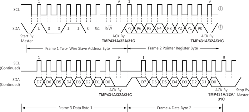
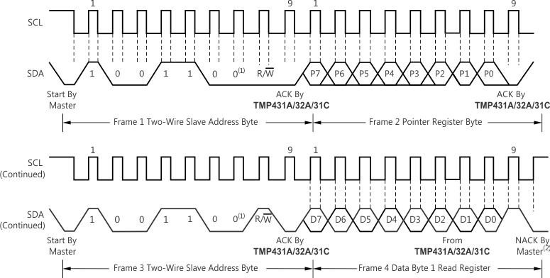
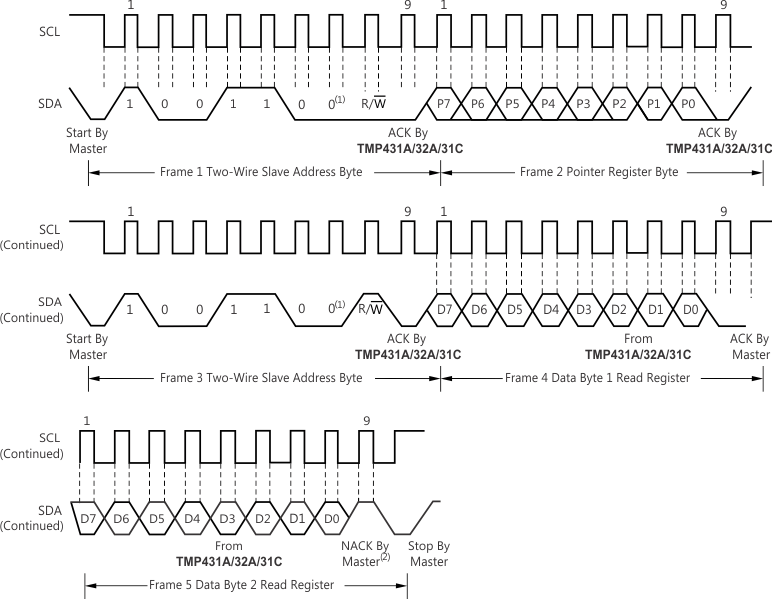
The TMP43x are Two-Wire and SMBus-compatible. Figure 13 to Figure 17 describe the various operations on the TMP43x. Parameters for Figure 13 are defined in Figure 14. Bus definitions are given below:

Bus Idle: Both SDA and SCL lines remain high.

Start Data Transfer: A change in the state of the SDA line from high to low when the SCL line is high defines a START condition. Each data transfer is initiated with a START condition.

Stop Data Transfer: A change in the state of the SDA line from low to high when the SCL line is high defines a STOP condition. Each data transfer terminates with a STOP or a repeated START condition.

Data Transfer: The number of data bytes transferred between a START and a STOP condition is not limited and is determined by the master device. The receiver acknowledges the transfer of data.

Acknowledge: Each receiving device, when addressed, is obliged to generate an Acknowledge bit. A device that acknowledges must pull down the SDA line during the Acknowledge clock pulse in such a way that the SDA line is stable low during the high period of the Acknowledge clock pulse. Setup and hold times must be taken into account. On a master receive, data transfer termination can be signaled by the master generating a Not-Acknowledge on the last byte that has been transmitted by the slave.

TMP431 TMP432 ai_tim_two-wire_bos441.gifFigure 13. Two-Wire Timing Diagram
TMP431 TMP432 ai_tim_two-wire_write_bos441.gif
Slave address 1001100 (TMP431A, 32A, and 31C) shown. Slave address changes for TMP431B, 32B, and 31D. See メカニカル、パッケージ、および注文情報 for more details.
Figure 14. Two-Wire Timing Diagram for Write Word Format
TMP431 TMP432 ai_tim_two-wire_one_read_bos441.gif
Slave address 1001100 (TMP431A, 32A, and 31C) shown. Slave address changes for TMP431B, 32B, and 31D. See メカニカル、パッケージ、および注文情報 for more details.
Master must leave SDA high to terminate a single-byte read operation.
Figure 15. Two-Wire Timing Diagram for Single-Byte Read Format
TMP431 TMP432 ai_tim_two-wire_two_read_bos441.gif
Slave address 1001100 (TMP431A, 32A, and 31C) shown. Slave address changes for TMP431B, 32B, and 31D. See メカニカル、パッケージ、および注文情報 for more details.
Master must leave SDA high to terminate a two-byte read operation.
Figure 16. Two-Wire Timing Diagram for Two-Byte Read Format
TMP431 TMP432 ai_tim_smbus_alert_bos441.gif
Slave address 1001100 (TMP431A, 32A, and 31C) shown. Slave address changes for TMP431B, 32B, and 31D. See メカニカル、パッケージ、および注文情報 for more details.
Figure 17. Timing Diagram for SMBus ALERT