JAJSGU6C October 2014 – April 2021 TMP451-Q1
PRODUCTION DATA
- 1 特長
- 2 アプリケーション
- 3 概要
- 4 Revision History
- 5 Pin Configuration and Functions
- 6 Specifications
-
7 Detailed Description
- 7.1 Overview
- 7.2 Functional Block Diagram
- 7.3 Feature Description
- 7.4 Device Functional Modes
- 7.5 Programming
- 7.6 Register Map
- 8 Application and Implementation
- 9 Power Supply Recommendations
- 10Layout
- 11Device and Documentation Support
- 12Mechanical, Packaging, and Orderable Information
パッケージ・オプション
メカニカル・データ(パッケージ|ピン)
サーマルパッド・メカニカル・データ
発注情報
10.1 Layout Guidelines
Remote temperature sensing on the TMP451-Q1 device measures very small voltages using very low currents; therefore, noise at the device inputs must be minimized. Most applications using the TMP451-Q1 have high digital content, with several clocks and logic level transitions creating a noisy environment. Layout should adhere to the following guidelines:
- Place the TMP451-Q1 device as close to the remote junction sensor as possible.
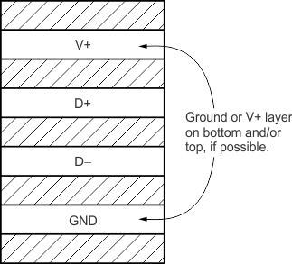
- Route the D+ and D– traces next to each other and shield them from adjacent signals through the use of ground guard traces; see Figure 10-1. If a multilayer PCB is used, bury these traces between ground or V+ planes to shield them from extrinsic noise sources. 5 mil (0.127 mm) PCB traces are recommended.
- Minimize additional thermocouple junctions caused by copper-to-solder connections. If these junctions are used, make the same number and approximate locations of copper-to-solder connections in both the D+ and D– connections to cancel any thermocouple effects.
- Use a 0.1μF local bypass capacitor directly between the V+ and GND of the TMP451-Q1 device. For optimum measurement performance, minimize filter capacitance between D+ and D– to 1000 pF or less . This capacitance includes any cable capacitance between the remote temperature sensor and the TMP451-Q1 device.
- If the connection between the remote temperature sensor and the TMP451-Q1 device is less than 8-in (20,32 cm) long, use a twisted-wire pair connection. For lengths greater than 8 in, use a twisted, shielded pair with the shield grounded as close to the TMP451-Q1 device as possible. Leave the remote sensor connection end of the shield wire open to avoid ground loops and 60-Hz pickup.
- Thoroughly clean and remove all flux residue in and around the pins of the TMP451-Q1 device to avoid temperature offset readings as a result of leakage paths between D+ and GND, or between D+ and V+.

Use minimum 5-mil (0.127 mm) traces with 5-mil spacing.
Figure 10-1 Suggested PCB Layer Cross-Section