JAJSJN1A May 2023 – September 2023 TMP4718
PRODUCTION DATA
- 1
- 1 特長
- 2 アプリケーション
- 3 概要
- 4 Revision History
- 5 Device Comparison
- 6 Pin Configuration and Functions
- 7 Specifications
-
8 Detailed Description
- 8.1 Overview
- 8.2 Functional Block Diagram
- 8.3
Feature Description
- 8.3.1 1.2-V Logic Compatible Inputs
- 8.3.2 Series Resistance Cancellation
- 8.3.3 Device Initialization, Resistor Decoding, and Default Temperature Conversion
- 8.3.4 Adjustable Default T_CRIT High-Temperature Limit
- 8.3.5 ALERT and T_CRIT Output
- 8.3.6 Fault Queue
- 8.3.7 Filtering
- 8.3.8 One-Shot Conversions
- 8.4 Device Functional Modes
- 8.5 Programming
- 8.6 Register Map
- 9 Application and Implementation
- 10Device and Documentation Support
- 11Mechanical, Packaging, and Orderable Information
6 Pin Configuration and Functions
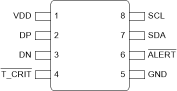
 Figure 6-1 DGK Package 8-Pin VSSOP (Top View)
Pin Functions
| PIN | I/O(1) | DESCRIPTION | |
|---|---|---|---|
| NAME | DGK | ||
| VDD | 1 | P | Supply Pin. Bypass to GND with a 0.1-μF capacitor. |
| DP | 2 | I/O | Positive connection to remote temperature sensors. Connect DP to DN if no remote diode is used. Place a 470-pF capacitor between DP and DN for noise filtering (if needed). |
| DN | 3 | I/O | Negative connection to remote temperature sensor. Connect DP to DN if no remote diode is used. Place a 470-pF capacitor between DP and DN for noise filtering (if needed). |
| T_CRIT | 4 | I/O | Open-drain critical temperature alert pin. A pullup resistor to VDD (or a separate bus) is required. The pullup resistor value is used to configure the default T_CRIT and ALERT high-temperature limits for the Remote and Local channels. See Adjustable Default T_CRIT High-Temperature Limit for more information. |
| GND | 5 | G | Ground connection |
| ALERT | 6 | I/O | Open-drain temperature alert pin. A pullup resistor to VDD (or a separate bus) is required. The pullup resistor value is used to configure the default T_CRIT and ALERT high-temperature limits for the Remote and Local channels. See Adjustable Default T_CRIT High-Temperature Limit for more information. |
| SDA | 7 | I/O | Open-drain serial data line. Requires a pullup resistor. |
| SCL | 8 | I | Open-drain serial clock Input line. Note I2C clock stretching is not supported. |
(1) I = Input, O = Output, I/O = Input or Output, G = Ground, P = Power.