JAJSJN1A May 2023 – September 2023 TMP4718
PRODUCTION DATA
- 1
- 1 特長
- 2 アプリケーション
- 3 概要
- 4 Revision History
- 5 Device Comparison
- 6 Pin Configuration and Functions
- 7 Specifications
-
8 Detailed Description
- 8.1 Overview
- 8.2 Functional Block Diagram
- 8.3
Feature Description
- 8.3.1 1.2-V Logic Compatible Inputs
- 8.3.2 Series Resistance Cancellation
- 8.3.3 Device Initialization, Resistor Decoding, and Default Temperature Conversion
- 8.3.4 Adjustable Default T_CRIT High-Temperature Limit
- 8.3.5 ALERT and T_CRIT Output
- 8.3.6 Fault Queue
- 8.3.7 Filtering
- 8.3.8 One-Shot Conversions
- 8.4 Device Functional Modes
- 8.5 Programming
- 8.6 Register Map
- 9 Application and Implementation
- 10Device and Documentation Support
- 11Mechanical, Packaging, and Orderable Information
8.5.4.2 Reads
For a read operation, the controller sends a START condition followed by the target address with the R/W bit set to 0 (signifying a write). The target acknowledges the write request, and the controller sends the Register Pointer. After the Register Pointer, the host will initiate a restart followed by the target address with the R/W bit set to 1 (signifying a read). The controller will continue to send out clock pulses but releases the SDA line so that the target can transmit data. At the end of every byte of data, the controller sends an ACK to the target, letting the target know that the controller is ready for more data. Figure 8-13 shows an example of reading a single byte from a target register. The TMP4718 does not support multiple register reads with a single transaction.
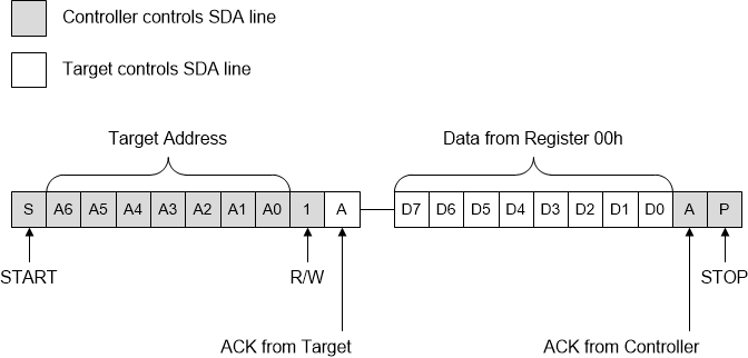
If repeated reads from the same register are desired, the pointer register bytes do not have to be continually sent, as shown in Figure 8-14. The TMP4718 remembers the pointer register value until the value is changed by the next write operation. Note after the device POR, the pointer address is defaulted to 0h. Therefore, the controller can read (and re-read) the Temp_Local register content without setting the pointer value.
 Figure 8-13 Read from Single Register
 Figure 8-14 Repeated Read from Single Register