JAJSJN1A May 2023 – September 2023 TMP4718
PRODUCTION DATA
- 1
- 1 特長
- 2 アプリケーション
- 3 概要
- 4 Revision History
- 5 Device Comparison
- 6 Pin Configuration and Functions
- 7 Specifications
-
8 Detailed Description
- 8.1 Overview
- 8.2 Functional Block Diagram
- 8.3
Feature Description
- 8.3.1 1.2-V Logic Compatible Inputs
- 8.3.2 Series Resistance Cancellation
- 8.3.3 Device Initialization, Resistor Decoding, and Default Temperature Conversion
- 8.3.4 Adjustable Default T_CRIT High-Temperature Limit
- 8.3.5 ALERT and T_CRIT Output
- 8.3.6 Fault Queue
- 8.3.7 Filtering
- 8.3.8 One-Shot Conversions
- 8.4 Device Functional Modes
- 8.5 Programming
- 8.6 Register Map
- 9 Application and Implementation
- 10Device and Documentation Support
- 11Mechanical, Packaging, and Orderable Information
8.5.2 I2C and SMBus Interface
The TMP4718 has a standard bidirectional I2C interface that can be configured or read by a controller. Each target on the I2C bus has a specific device address to differentiate between other target devices that are on the same I2C bus. Many target devices require configuration upon start-up to set the behavior of the device. This is typically done when the controller accesses internal register maps of the target, which have unique register addresses. A device can have one or multiple registers where data is stored, written, or read. The TMP4718 includes 50-ns glitch suppression filters, allowing the device to coexist on I3C mixed bus.
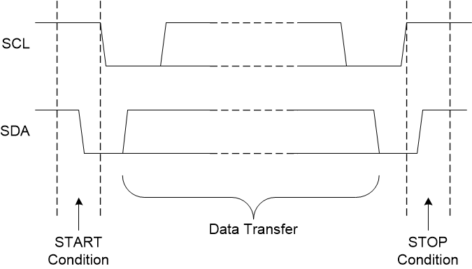
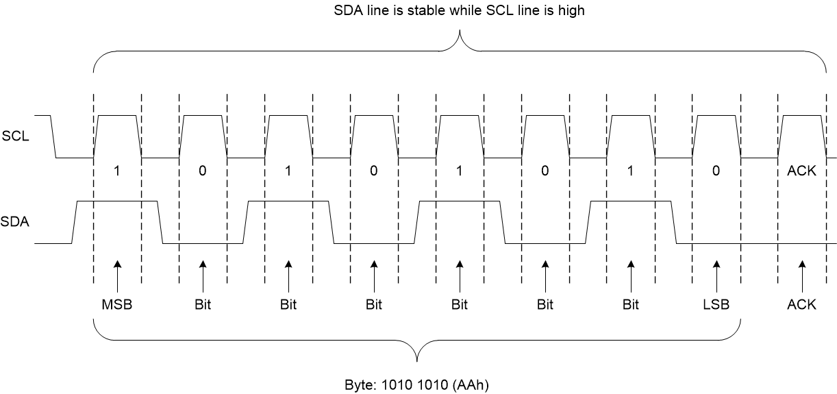
The physical I2C interface consists of the serial clock (SCL) and serial data (SDA) lines. Both SDA and SCL lines must be connected to a supply through a pullup resistor. The size of the pullup resistor is determined by the amount of capacitance on the I2C lines. See also the I2C Bus Pullup Resistor Calculation application note. Data transfer may be initiated only when the bus is idle. A bus is considered idle if both SDA and SCL lines are high after a STOP condition (see Figure 8-10 and Figure 8-11). See the Adjustable Default T_CRIT High-Temperature LimitAdjustable Default T_CRIT High-Temperature LimitFault QueueOne-Shot ConversionsInterrupt and Comparator ModeShutdown ModeContinuous Conversion ModeProgrammingTemperature Data FormatI2C and SMBus InterfaceDevice AddressBus TransactionsWritesReadsAdjustable Default T_CRIT High-Temperature Limit and Adjustable Default T_CRIT High-Temperature LimitAdjustable Default T_CRIT High-Temperature LimitFault QueueOne-Shot ConversionsInterrupt and Comparator ModeShutdown ModeContinuous Conversion ModeProgrammingTemperature Data FormatI2C and SMBus InterfaceDevice AddressBus TransactionsWritesReadsAdjustable Default T_CRIT High-Temperature Limit sections for detail procedures on how the controller can access the TMP4718.
 Figure 8-10 Definition of Start and Stop Conditions
 Figure 8-11 Bit Transfer