JAJSTJ4A June 2022 – March 2024 TMS570LC4357-SEP
PRODUCTION DATA
- 1
- 1 特長
- 2 アプリケーション
- 3 概要
- 4 Device Comparison
-
5 Terminal Configuration and Functions
- 5.1 GWT BGA Package Ball-Map (337 Terminal Grid Array)
- 5.2
Terminal Functions
- 5.2.1
GWT Package
- 5.2.1.1 Multibuffered Analog-to-Digital Converters (MibADC)
- 5.2.1.2 Enhanced High-End Timer Modules (N2HET)
- 5.2.1.3 RAM Trace Port (RTP)
- 5.2.1.4 Enhanced Capture Modules (eCAP)
- 5.2.1.5 Enhanced Quadrature Encoder Pulse Modules (eQEP)
- 5.2.1.6 Enhanced Pulse-Width Modulator Modules (ePWM)
- 5.2.1.7 Data Modification Module (DMM)
- 5.2.1.8 General-Purpose Input / Output (GIO)
- 5.2.1.9 FlexRay Interface Controller (FlexRay)
- 5.2.1.10 Controller Area Network Controllers (DCAN)
- 5.2.1.11 Local Interconnect Network Interface Module (LIN)
- 5.2.1.12 Standard Serial Communication Interface (SCI)
- 5.2.1.13 Inter-Integrated Circuit Interface Module (I2C)
- 5.2.1.14 Multibuffered Serial Peripheral Interface Modules (MibSPI)
- 5.2.1.15 Ethernet Controller
- 5.2.1.16 External Memory Interface (EMIF)
- 5.2.1.17 Embedded Trace Macrocell Interface for Cortex-R5F (ETM-R5)
- 5.2.1.18 System Module Interface
- 5.2.1.19 Clock Inputs and Outputs
- 5.2.1.20 Test and Debug Modules Interface
- 5.2.1.21 Flash Supply and Test Pads
- 5.2.1.22 Supply for Core Logic: 1.2-V Nominal
- 5.2.1.23 Supply for I/O Cells: 3.3-V Nominal
- 5.2.1.24 Ground Reference for All Supplies Except VCCAD
- 5.2.1.25 Other Supplies
- 5.2.2 Multiplexing
- 5.2.1
GWT Package
-
6 Specifications
- 6.1 Absolute Maximum Ratings
- 6.2 ESD Ratings
- 6.3 Power-On Hours (POH)
- 6.4 Recommended Operating Conditions
- 6.5 Switching Characteristics Over Recommended Operating Conditions for Clock Domains
- 6.6 Wait States Required - L2 Memories
- 6.7 Power Consumption Summary
- 6.8 Input/Output Electrical Characteristics Over Recommended Operating Conditions
- 6.9 Thermal Resistance Characteristics for the BGA Package (GWT)
- 6.10 Timing and Switching Characteristics
-
7 System Information and Electrical Specifications
- 7.1 Device Power Domains
- 7.2 Voltage Monitor Characteristics
- 7.3 Power Sequencing and Power-On Reset
- 7.4 Warm Reset (nRST)
- 7.5 Arm Cortex-R5F CPU Information
- 7.6 Clocks
- 7.7 Clock Monitoring
- 7.8 Glitch Filters
- 7.9 Device Memory Map
- 7.10 Flash Memory
- 7.11 L2RAMW (Level 2 RAM Interface Module)
- 7.12 ECC / Parity Protection for Accesses to Peripheral RAMs
- 7.13 On-Chip SRAM Initialization and Testing
- 7.14 External Memory Interface (EMIF)
- 7.15 Vectored Interrupt Manager
- 7.16 ECC Error Event Monitoring and Profiling
- 7.17 DMA Controller
- 7.18 Real-Time Interrupt Module
- 7.19 Error Signaling Module
- 7.20 Reset / Abort / Error Sources
- 7.21 Digital Windowed Watchdog
- 7.22
Debug Subsystem
- 7.22.1 Block Diagram
- 7.22.2 Debug Components Memory Map
- 7.22.3 Embedded Cross Trigger
- 7.22.4 JTAG Identification Code
- 7.22.5 Debug ROM
- 7.22.6 JTAG Scan Interface Timings
- 7.22.7 Advanced JTAG Security Module
- 7.22.8 Embedded Trace Macrocell (ETM-R5)
- 7.22.9 RAM Trace Port (RTP)
- 7.22.10 Data Modification Module (DMM)
- 7.22.11 Boundary Scan Chain
-
8 Peripheral Information and Electrical Specifications
- 8.1
Enhanced Translator PWM Modules (ePWM)
- 8.1.1 ePWM Clocking and Reset
- 8.1.2 Synchronization of ePWMx Time-Base Counters
- 8.1.3 Synchronizing all ePWM Modules to the N2HET1 Module Time Base
- 8.1.4 Phase-Locking the Time-Base Clocks of Multiple ePWM Modules
- 8.1.5 ePWM Synchronization with External Devices
- 8.1.6 ePWM Trip Zones
- 8.1.7 Triggering of ADC Start of Conversion Using ePWMx SOCA and SOCB Outputs
- 8.1.8 Enhanced Translator-Pulse Width Modulator (ePWMx) Electrical Data/Timing
- 8.2 Enhanced Capture Modules (eCAP)
- 8.3 Enhanced Quadrature Encoder (eQEP)
- 8.4 12-bit Multibuffered Analog-to-Digital Converter (MibADC)
- 8.5 General-Purpose Input/Output
- 8.6 Enhanced High-End Timer (N2HET)
- 8.7 FlexRay Interface
- 8.8 Controller Area Network (DCAN)
- 8.9 Local Interconnect Network Interface (LIN)
- 8.10 Serial Communication Interface (SCI)
- 8.11 Inter-Integrated Circuit (I2C)
- 8.12 Multibuffered / Standard Serial Peripheral Interface
- 8.13 Ethernet Media Access Controller
- 8.1
Enhanced Translator PWM Modules (ePWM)
- 9 Applications, Implementation, and Layout
- 10Device and Documentation Support
- 11Revision History
- 12Mechanical, Packaging, and Orderable Information
パッケージ・オプション
デバイスごとのパッケージ図は、PDF版データシートをご参照ください。
メカニカル・データ(パッケージ|ピン)
- GWT|337
サーマルパッド・メカニカル・データ
発注情報
7.22.3 Embedded Cross Trigger
The Embedded Cross Trigger (ECT) is a modular component that supports the interaction and synchronization of multiple triggering events within a SoC.
The ECT consists of two modules:
- A (Cross Trigger Interface) CTI. The CTI provides the interface between a component or subsystem and the Cross Trigger Matrix (CTM).
- A CTM. The CTM combines the trigger requests generated from CTIs and broadcasts them to all CTIs as channel triggers. This enables subsystems to interact, cross trigger, with one another.
 Figure 7-24 CTI/CTM Integration
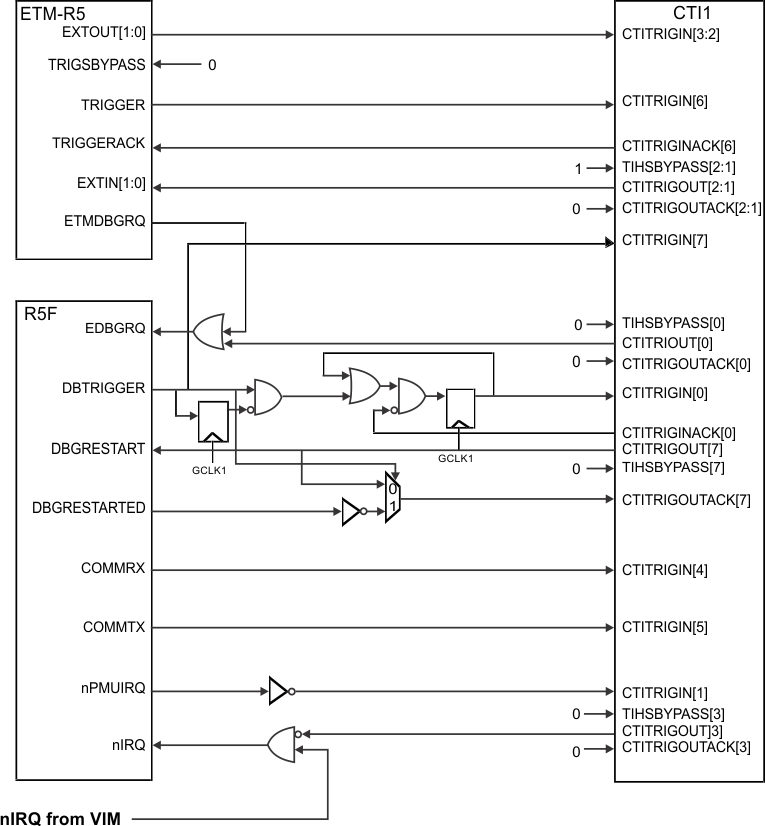
 Figure 7-25 CTI1 Mapping
Note:
ETM-R5, Cortex-R5F and CTI1 run at same frequency.
Table 7-48 CTI1 Mapping
| CTI TRIGGER | Module Signal |
|---|---|
| Trigger Input 0 | From Cortex-R5F DBTRIGGER |
| Trigger Input 1 | From Cortex-R5F nPMUIRQ |
| Trigger Input 2 | From ETM-R5 EXTOUT[0] |
| Trigger Input 3 | From ETM-R5 EXTOUT[1] |
| Trigger Input 4 | From Cortex-R5F COMMRX |
| Trigger Input 5 | From Cortex-R5F COMMTX |
| Trigger Input 6 | From ETM-R5 TRIGGER |
| Trigger Input 7 | From Cortex-R5F DBTRIGGER |
| Trigger Output 0 | To Cortex-R5F EDBGRQ |
| Trigger Output 1 | To ETM-R5 EXTIN[0] |
| Trigger Output 2 | To ETM-R5 EXTIN[1] |
| Trigger Output 3 | To Cortex-R5F nIRQ |
| Trigger Output 4 | Reserved |
| Trigger Output 5 | Reserved |
| Trigger Output 6 | Reserved |
| Trigger Output 7 | To Cortex-R5F DBGRESTARTED |
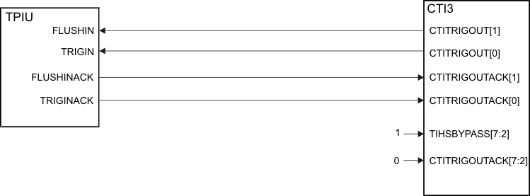
 Figure 7-26 CTI3 Mapping
Note:
TPIU and CTI3 run at different frequencies.
Table 7-49 CTI3 Mapping
| CTI TRIGGER | Module Signal |
|---|---|
| Trigger Input 0 | Reserved |
| Trigger Input 1 | Reserved |
| Trigger Input 2 | Reserved |
| Trigger Input 3 | Reserved |
| Trigger Input 4 | Reserved |
| Trigger Input 5 | Reserved |
| Trigger Input 6 | Reserved |
| Trigger Input 7 | Reserved |
| Trigger Output 0 | To TPIU TRIGIN |
| Trigger Output 1 | To TPIU FLUSHIN |
| Trigger Output 2 | Reserved |
| Trigger Output 3 | Reserved |
| Trigger Output 4 | Reserved |
| Trigger Output 5 | Reserved |
| Trigger Output 6 | Reserved |
| Trigger Output 7 | Reserved |
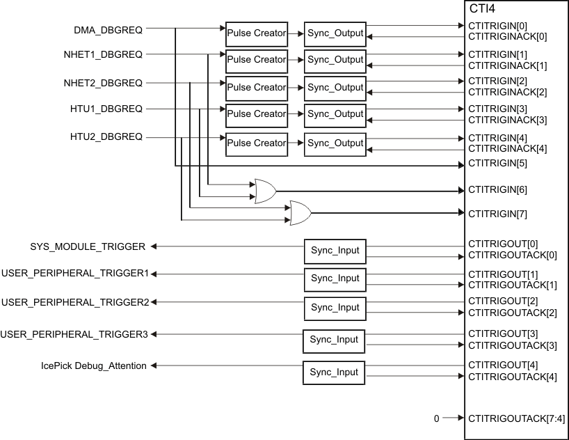
 Figure 7-27 CTI4 Mapping
Table 7-50 CTI4 Mapping
| CTI TRIGGER | Module Signal |
|---|---|
| Trigger Input 0 | From DMA_DBGREQ |
| Trigger Input 1 | From N2HET1_DBGREQ |
| Trigger Input 2 | From N2HET2_DBGREQ |
| Trigger Input 3 | From HTU1_DBGREQ |
| Trigger Input 4 | From HTU2_DBGREQ |
| Trigger Input 5 | From DMA_DBGREQ |
| Trigger Input 6 | From N2HET1_DBGREQ or HTU1_DBGREQ |
| Trigger Input 7 | From N2HET2_DBGREQ or HTU2_DBGREQ |
| Trigger Output 0 | To SYS_MODULE_TRIGGER |
| Trigger Output 1 | To USER_PERIPHERAL_TRIGGER1 |
| Trigger Output 2 | To USER_PERIPHERAL_TRIGGER2 |
| Trigger Output 3 | To USER_PERIPHERAL_TRIGGER3 |
| Trigger Output 4 | To IcePick Debug_Attention |
| Trigger Output 5 | Reserved |
| Trigger Output 6 | Reserved |
| Trigger Output 7 | Reserved |
Table 7-51 Peripheral Suspend Generation
| TRIGGER OUTPUT | MODULE SIGNAL CONNECTED | DESCRIPTION |
|---|---|---|
| SYS_MODULE_TRIGGER | L2FMC_CPU_EMUSUSP | L2FMC Wrapper Suspend |
| CCM_R5_CPU_EMUSUSP | CCM_R5 module suspend | |
| CRC_CPU_EMUSUSP | CRC1 / CRC2 module suspend | |
| SYS_CPU_EMUSUSP | SYS module Suspend | |
| USER_PERIPHERAL_TRIGGER1 | DMA_SUSPEND | DMA Suspend |
| RTI_CPU_SUSPEND | RTI1 / RTI2 Suspend | |
| AWM_CPU_SUSPEND | AWM1 / AWM2 Suspend | |
| HTU_CPU_EMUSUSP | HTU1 / HTU2 Suspend | |
| SCI_CPU_EMUSUSP | SCI3 / SCI4 Suspend | |
| LIN_CPU_EMUSUSP | LIN1 / LIN2 Suspend | |
| I2C_CPU_EMUSUSP | I2C1 / I2C2 Suspend | |
| EMAC_CPU_EMUSUSP | EMAC Suspend | |
| EQEP_CPU_EMUSUSP | EQEP Suspend | |
| ECAP_CPU_EMUSUSP | ECAP Suspend | |
| DMM_CPU_EMUSUSP | DMM Suspend | |
| DCC_CPU_EMUSUSP | DCC1 / DCC2 Suspend | |
| USER_PERIPHERAL_TRIGGER2 | DCAN_CPU_EMUSUSP | DCAN1 / DCAN2 / DCAN3 / DCAN4 Suspend |
| USER_PERIPHERAL_TRIGGER3 | ePWM_CPU_EMUSUSP | ePWM1..7 Trip Zone TZ6n and ePWM1..7 Suspend |