JAJSFJ6C October 2012 – May 2018 TMS570LS0332 , TMS570LS0432
PRODUCTION DATA.
- 1デバイスの概要
- 2改訂履歴
- 3Device Comparison
-
4Terminal Configuration and Functions
- 4.1 PZ QFP Package Pinout (100-Pin)
- 4.2
Terminal Functions
- 4.2.1 High-End Timer (N2HET)
- 4.2.2 Enhanced Quadrature Encoder Pulse Modules (eQEP)
- 4.2.3 General-Purpose Input/Output (GPIO)
- 4.2.4 Controller Area Network Interface Modules (DCAN1, DCAN2)
- 4.2.5 Multibuffered Serial Peripheral Interface (MibSPI1)
- 4.2.6 Standard Serial Peripheral Interface (SPI2)
- 4.2.7 Local Interconnect Network Controller (LIN)
- 4.2.8 Multibuffered Analog-to-Digital Converter (MibADC)
- 4.2.9 System Module
- 4.2.10 Error Signaling Module (ESM)
- 4.2.11 Main Oscillator
- 4.2.12 Test/Debug Interface
- 4.2.13 Flash
- 4.2.14 Core Supply
- 4.2.15 I/O Supply
- 4.2.16 Core and I/O Supply Ground Reference
- 4.3 Output Multiplexing and Control
- 4.4 Special Multiplexed Options
-
5Specifications
- 5.1 Absolute Maximum Ratings
- 5.2 ESD Ratings
- 5.3 Power-On Hours (POH)
- 5.4 Recommended Operating Conditions
- 5.5 Switching Characteristics Over Recommended Operating Conditions for Clock Domains
- 5.6 Wait States Required
- 5.7 Power Consumption
- 5.8 Thermal Resistance Characteristics for PZ
- 5.9 Input/Output Electrical Characteristics
- 5.10 Output Buffer Drive Strengths
- 5.11 Input Timings
- 5.12 Output Timings
-
6System Information and Electrical Specifications
- 6.1 Voltage Monitor Characteristics
- 6.2 Power Sequencing and Power-On Reset
- 6.3 Warm Reset (nRST)
- 6.4 ARM Cortex-R4 CPU Information
- 6.5 Clocks
- 6.6 Clock Monitoring
- 6.7 Glitch Filters
- 6.8 Device Memory Map
- 6.9 Flash Memory
- 6.10 Flash Program and Erase Timings for Program Flash
- 6.11 Flash Program and Erase Timings for Data Flash
- 6.12 Tightly Coupled RAM Interface Module
- 6.13 Parity Protection for Accesses to peripheral RAMs
- 6.14 On-Chip SRAM Initialization and Testing
- 6.15 Vectored Interrupt Manager
- 6.16 Real-Time Interrupt Module
- 6.17 Error Signaling Module
- 6.18 Reset / Abort / Error Sources
- 6.19 Digital Windowed Watchdog
- 6.20 Debug Subsystem
-
7Peripheral Information and Electrical Specifications
- 7.1 Peripheral Legend
- 7.2 Multibuffered 12-Bit Analog-to-Digital Converter
- 7.3 General-Purpose Input/Output
- 7.4 Enhanced High-End Timer (N2HET)
- 7.5 Controller Area Network (DCAN)
- 7.6 Local Interconnect Network Interface (LIN)
- 7.7 Multibuffered / Standard Serial Peripheral Interface
- 7.8 Enhanced Quadrature Encoder (eQEP)
- 8デバイスおよびドキュメントのサポート
- 9メカニカル、パッケージ、および注文に関する付録
パッケージ・オプション
メカニカル・データ(パッケージ|ピン)
- PZ|100
サーマルパッド・メカニカル・データ
- PZ|100
発注情報
7.7.5 SPI Slave Mode I/O Timings
Table 7-15 SPI Slave Mode External Timing Parameters (CLOCK PHASE = 0, SPICLK = input, SPISIMO = input, and SPISOMI = output)(1)(2)(3)(4)
| NO. | PARAMETER | MIN | MAX | UNIT | |
|---|---|---|---|---|---|
| 1 | tc(SPC)S | Cycle time, SPICLK(5) | 40 | ns | |
| 2(6) | tw(SPCH)S | Pulse duration, SPICLK high (clock polarity = 0) | 14 | ns | |
| tw(SPCL)S | Pulse duration, SPICLK low (clock polarity = 1) | 14 | |||
| 3(6) | tw(SPCL)S | Pulse duration, SPICLK low (clock polarity = 0) | 14 | ns | |
| tw(SPCH)S | Pulse duration, SPICLK high (clock polarity = 1) | 14 | |||
| 4(6) | td(SPCH-SOMI)S | Delay time, SPISOMI valid after SPICLK high (clock polarity = 0) | trf(SOMI) + 20 | ns | |
| td(SPCL-SOMI)S | Delay time, SPISOMI valid after SPICLK low (clock polarity = 1) | trf(SOMI) + 20 | |||
| 5(6) | th(SPCH-SOMI)S | Hold time, SPISOMI data valid after SPICLK high (clock polarity =0) | 2 | ns | |
| th(SPCL-SOMI)S | Hold time, SPISOMI data valid after SPICLK low (clock polarity =1) | 2 | |||
| 6(6) | tsu(SIMO-SPCL)S | Setup time, SPISIMO before SPICLK low (clock polarity = 0) | 4 | ns | |
| tsu(SIMO-SPCH)S | Setup time, SPISIMO before SPICLK high (clock polarity = 1) | 4 | |||
| 7(6) | th(SPCL-SIMO)S | Hold time, SPISIMO data valid after SPICLK low (clock polarity = 0) | 2 | ns | |
| th(SPCH-SIMO)S | Hold time, SPISIMO data valid after S PICLK high (clock polarity = 1) | 2 | |||
| 8 | td(SPCL-SENAH)S | Delay time, SPIENAn high after last SPICLK low (clock polarity = 0) | 1.5tc(VCLK) | 2.5tc(VCLK)+tr(ENAn)+ 22 | ns |
| td(SPCH-SENAH)S | Delay time, SPIENAn high after last SPICLK high (clock polarity = 1) | 1.5tc(VCLK) | 2.5tc(VCLK)+ tr(ENAn) + 22 | ||
| 9 | td(SCSL-SENAL)S | Delay time, SPIENAn low after SPICSn low (if new data has been written to the SPI buffer) | tf(ENAn) | tc(VCLK)+tf(ENAn)+27 | ns |
(1) The MASTER bit (SPIGCR1.0) is cleared and the CLOCK PHASE bit (SPIFMTx.16) is cleared.
(2) If the SPI is in slave mode, the following must be true: tc(SPC)S ≥ (PS + 1) tc(VCLK), where PS = prescale value set in SPIFMTx.[15:8].
(3) For rise and fall timings, see Table 5-6.
(4) tc(VCLK) = interface clock cycle time = 1 /f(VCLK)
(5) When the SPI is in Slave mode, the following must be true:
For PS values from 1 to 255: tc(SPC)S ≥ (PS +1)tc(VCLK) ≥ 40 ns, where PS is the prescale value set in the SPIFMTx.[15:8] register bits.
For PS values of 0: tc(SPC)S = 2tc(VCLK) ≥ 40 ns.
For PS values from 1 to 255: tc(SPC)S ≥ (PS +1)tc(VCLK) ≥ 40 ns, where PS is the prescale value set in the SPIFMTx.[15:8] register bits.
For PS values of 0: tc(SPC)S = 2tc(VCLK) ≥ 40 ns.
(6) The active edge of the SPICLK signal referenced is controlled by the CLOCK POLARITY bit (SPIFMTx.17).
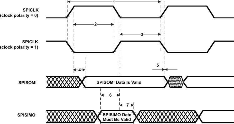
 Figure 7-10 SPI Slave Mode External Timing (CLOCK PHASE = 0)
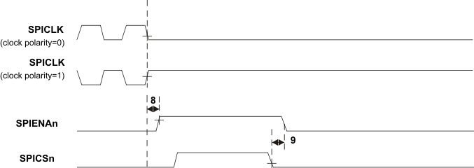
  Figure 7-11 SPI Slave Mode Enable Timing (CLOCK PHASE = 0)
 Table 7-16 SPI Slave Mode External Timing Parameters (CLOCK PHASE = 1, SPICLK = input, SPISIMO = input, and SPISOMI = output)(1)(2)(3)(4)
| NO. | PARAMETER | MIN | MAX | UNIT | |
|---|---|---|---|---|---|
| 1 | tc(SPC)S | Cycle time, SPICLK(5) | 40 | ns | |
| 2(6) | tw(SPCH)S | Pulse duration, SPICLK high (clock polarity = 0) | 14 | ns | |
| tw(SPCL)S | Pulse duration, SPICLK low (clock polarity = 1) | 14 | |||
| 3(6) | tw(SPCL)S | Pulse duration, SPICLK low (clock polarity = 0) | 14 | ns | |
| tw(SPCH)S | Pulse duration, SPICLK high (clock polarity = 1) | 14 | |||
| 4(6) | td(SOMI-SPCL)S | Dealy time, SPISOMI data valid after SPICLK low (clock polarity = 0) | trf(SOMI) + 20 | ns | |
| td(SOMI-SPCH)S | Delay time, SPISOMI data valid after SPICLK high (clock polarity = 1) | trf(SOMI) + 20 | |||
| 5(6) | th(SPCL-SOMI)S | Hold time, SPISOMI data valid after SPICLK high (clock polarity =0) | 2 | ns | |
| th(SPCH-SOMI)S | Hold time, SPISOMI data valid after SPICLK low (clock polarity =1) | 2 | |||
| 6(6) | tsu(SIMO-SPCH)S | Setup time, SPISIMO before SPICLK high (clock polarity = 0) | 4 | ns | |
| tsu(SIMO-SPCL)S | Setup time, SPISIMO before SPICLK low (clock polarity = 1) | 4 | |||
| 7(6) | tv(SPCH-SIMO)S | High time, SPISIMO data valid after SPICLK high (clock polarity = 0) | 2 | ns | |
| tv(SPCL-SIMO)S | High time, SPISIMO data valid after SPICLK low (clock polarity = 1) | 2 | |||
| 8 | td(SPCH-SENAH)S | Delay time, SPIENAn high after last SPICLK high (clock polarity = 0) | 1.5tc(VCLK) | 2.5tc(VCLK)+tr(ENAn) + 22 | ns |
| td(SPCL-SENAH)S | Delay time, SPIENAn high after last SPICLK low (clock polarity = 1) | 1.5tc(VCLK) | 2.5tc(VCLK)+tr(ENAn) + 22 | ||
| 9 | td(SCSL-SENAL)S | Delay time, SPIENAn low after SPICSn low (if new data has been written to the SPI buffer) | tf(ENAn) | tc(VCLK)+tf(ENAn)+ 27 | ns |
| 10 | td(SCSL-SOMI)S | Delay time, SOMI valid after SPICSn low (if new data has been written to the SPI buffer) | tc(VCLK) | 2tc(VCLK)+trf(SOMI)+ 28 | ns |
(1) The MASTER bit (SPIGCR1.0) is cleared and the CLOCK PHASE bit (SPIFMTx.16) is set.
(2) If the SPI is in slave mode, the following must be true: tc(SPC)S ≤ (PS + 1) tc(VCLK), where PS = prescale value set in SPIFMTx.[15:8].
(3) For rise and fall timings, see Table 5-6.
(4) tc(VCLK) = interface clock cycle time = 1 /f(VCLK)
(5) When the SPI is in Slave mode, the following must be true:
For PS values from 1 to 255: tc(SPC)S ≥ (PS +1)tc(VCLK) ≥ 40 ns, where PS is the prescale value set in the SPIFMTx.[15:8] register bits.
For PS values of 0: tc(SPC)S = 2tc(VCLK) ≥ 40 ns.
For PS values from 1 to 255: tc(SPC)S ≥ (PS +1)tc(VCLK) ≥ 40 ns, where PS is the prescale value set in the SPIFMTx.[15:8] register bits.
For PS values of 0: tc(SPC)S = 2tc(VCLK) ≥ 40 ns.
(6) The active edge of the SPICLK signal referenced is controlled by the CLOCK POLARITY bit (SPIFMTx.17).
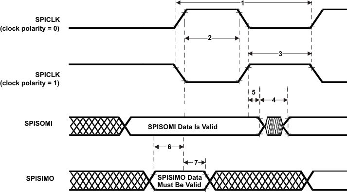
 Figure 7-12 SPI Slave Mode External Timing (CLOCK PHASE = 1)
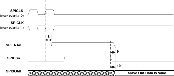
  Figure 7-13 SPI Slave Mode Enable Timing (CLOCK PHASE = 1)