JAJSHN8B June   2019  – January 2024 TMUX1133 , TMUX1134

PRODUCTION DATA  

  1.   1
  2. 特長
  3. アプリケーション
  4. 概要
  5. Device Comparison Table
  6. Pin Configuration and Functions
  7. Specifications
    1. 6.1  Absolute Maximum Ratings
    2. 6.2  ESD Ratings
    3. 6.3  Recommended Operating Conditions
    4. 6.4  Thermal Information
    5. 6.5  Electrical Characteristics (VDD = 5V ±10 %)
    6. 6.6  Electrical Characteristics (VDD = 3.3V ±10 %)
    7. 6.7  Electrical Characteristics (VDD = 2.5V ±10 %), (VSS = –2.5V ±10 %)
    8. 6.8  Electrical Characteristics (VDD = 1.8V ±10 %)
    9. 6.9  Electrical Characteristics (VDD = 1.2V ±10 %)
    10. 6.10 Typical Characteristics
  8. Parameter Measurement Information
    1. 7.1  On-Resistance
    2. 7.2  Off-Leakage Current
    3. 7.3  On-Leakage Current
    4. 7.4  Transition Time
    5. 7.5  Break-Before-Make
    6. 7.6  tON(EN) and tOFF(EN)
    7. 7.7  Charge Injection
    8. 7.8  Off Isolation
    9. 7.9  Crosstalk
    10. 7.10 Bandwidth
  9. Detailed Description
    1. 8.1 Overview
    2. 8.2 Functional Block Diagram
    3. 8.3 Feature Description
      1. 8.3.1 Bidirectional Operation
      2. 8.3.2 Rail to Rail Operation
      3. 8.3.3 1.8V Logic Compatible Inputs
      4. 8.3.4 Fail-Safe Logic
      5. 8.3.5 Ultra-low Leakage Current
      6. 8.3.6 Ultra-Low Charge Injection
    4. 8.4 Device Functional Modes
    5. 8.5 Truth Tables
  10. Application and Implementation
    1. 9.1 Application Information
    2. 9.2 Typical Application
      1. 9.2.1 Design Requirements
      2. 9.2.2 Detailed Design Procedure
      3. 9.2.3 Application Curve
    3. 9.3 Power Supply Recommendations
    4. 9.4 Layout
      1. 9.4.1 Layout Guidelines
      2. 9.4.2 Layout Example
  11. 10Device and Documentation Support
    1. 10.1 Documentation Support
      1. 10.1.1 Related Documentation
    2. 10.2 ドキュメントの更新通知を受け取る方法
    3. 10.3 サポート・リソース
    4. 10.4 Trademarks
    5. 10.5 静電気放電に関する注意事項
    6. 10.6 用語集
  12. 11Revision History
  13. 12Mechanical, Packaging, and Orderable Information

パッケージ・オプション

メカニカル・データ(パッケージ|ピン)
サーマルパッド・メカニカル・データ
発注情報

Typical Characteristics

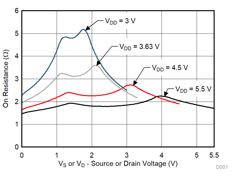
at TA = 25°C, VDD = 5V (unless otherwise noted)
GUID-5C06BDF3-E674-481F-B762-BEA9CBBA14B1-low.gif
TA = 25°C
Figure 6-1 On-Resistance vs Source or Drain Voltage
GUID-203218D8-551C-4A84-9955-1D9AEC715130-low.gif
VDD = ±2.5V
Figure 6-3 On-Resistance vs Temperature
GUID-0E86BA30-4A5B-47D3-92CE-CB46B1C927ED-low.gif
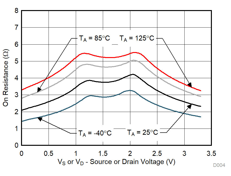
TA = 25°C
Figure 6-5 On-Resistance vs Source or Drain Voltage
GUID-2A06BB58-D6CB-43D6-9C61-D3AD1803CEE0-low.gif
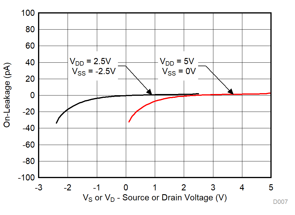
VDD = 5V
Figure 6-7 On-Leakage vs Source or Drain Voltage
GUID-DD013879-5929-49A5-BAE8-20F01D8A6294-low.gif
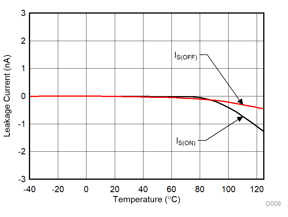
VDD = 5V
Figure 6-9 Leakage Current vs Temperature
GUID-A4D9F24D-E9CC-45E3-8A1A-9029161B4AB0-low.gif
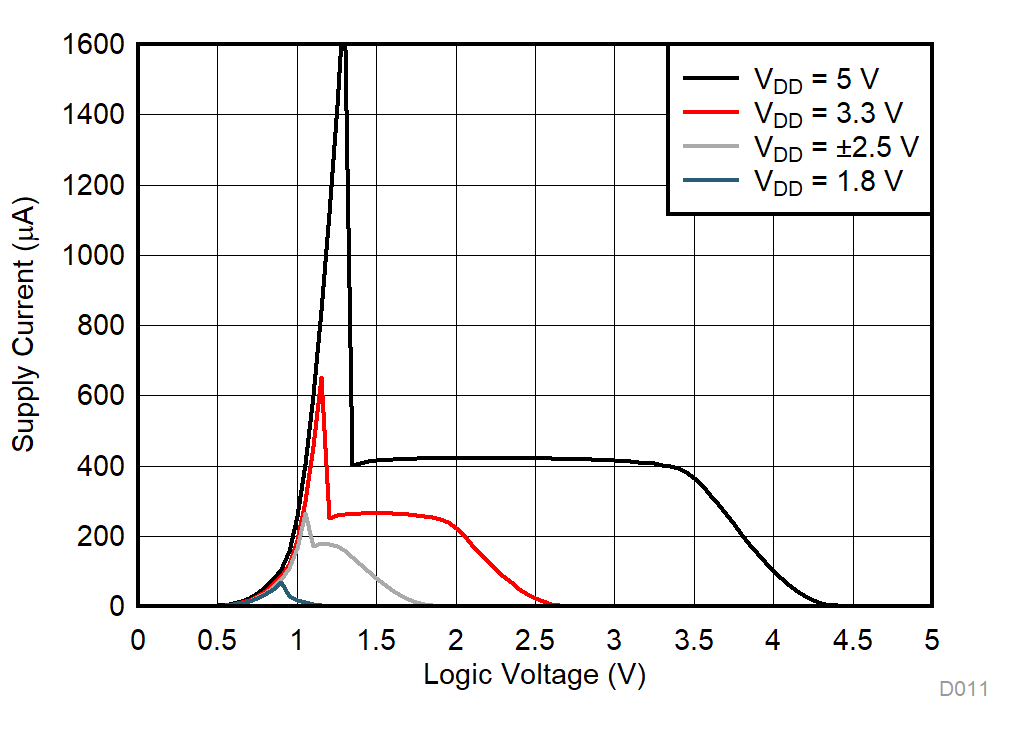
TA = 25°C
Figure 6-11 Supply Current vs Logic Voltage
GUID-9D1EA564-CA91-420C-8727-0E246F72CD47-low.gif
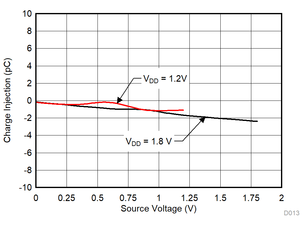
TA = -40°C to 125°C
Figure 6-13 Charge Injection vs Source Voltage
GUID-1503177C-49B4-4D8F-B10D-49F656FE2A5C-low.gif
TA = -40°C to +125°C
Figure 6-15 On Response vs Frequency
GUID-11311E13-D3A7-4FAB-8DEB-4588661ABD7F-low.gif
VDD = 5V
Figure 6-2 On-Resistance vs Temperature
GUID-785051E2-DD34-426B-B087-45CC5E5E8EA7-low.gif
VDD = 3.3V
Figure 6-4 On-Resistance vs Temperature
GUID-799F1566-6D0F-4E1A-9156-93A6D6EDEC33-low.gif
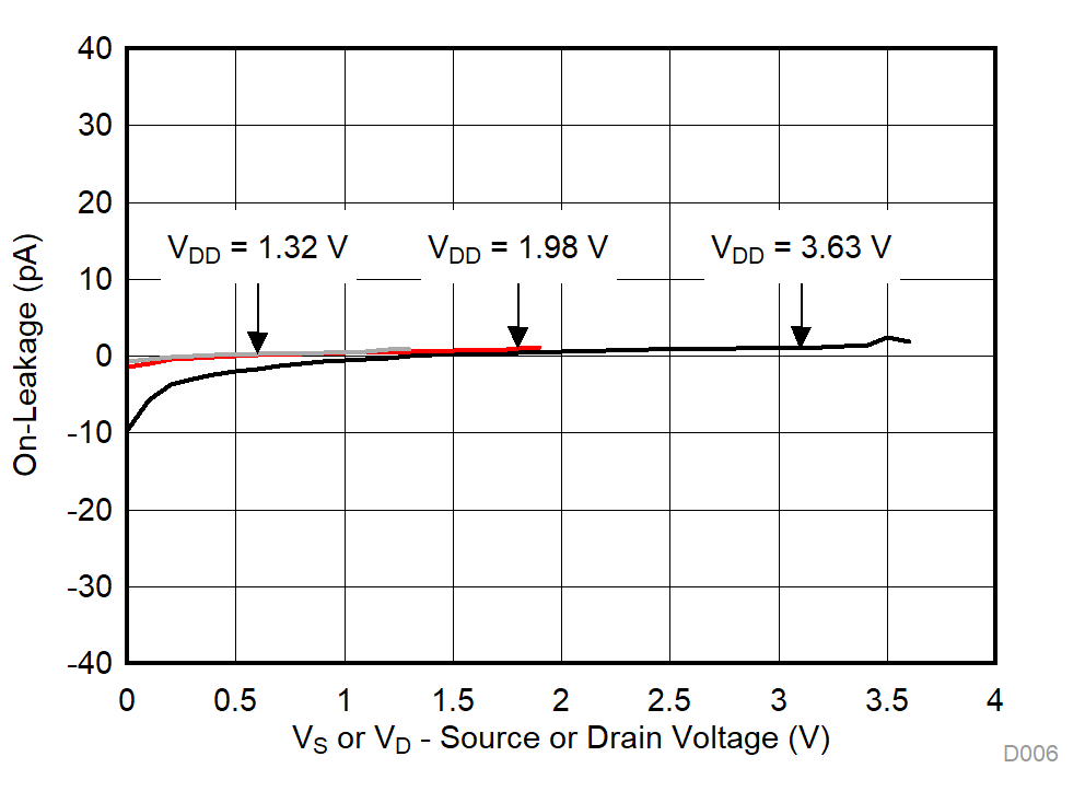
TA = 25°C
Figure 6-6 On-Leakage vs Source or Drain Voltage
GUID-0CCBCC1A-365C-47A5-A56A-BF756C627D3A-low.gif
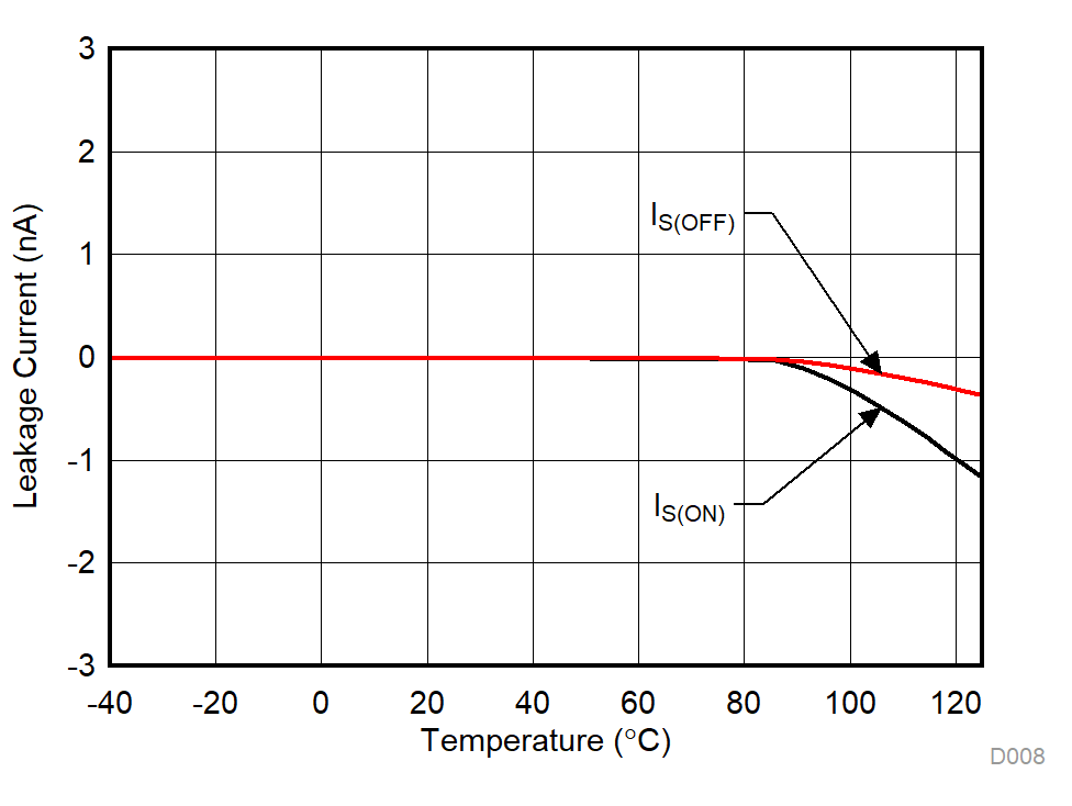
VDD = 3.3V
Figure 6-8 Leakage Current vs Temperature
GUID-908D7E10-586D-4780-BF23-8306051CA28E-low.gif
VSEL = VDD
Figure 6-10 Supply Current vs Temperature
GUID-977B8F5B-5A08-4583-8BE9-CD4305FACFAD-low.gif
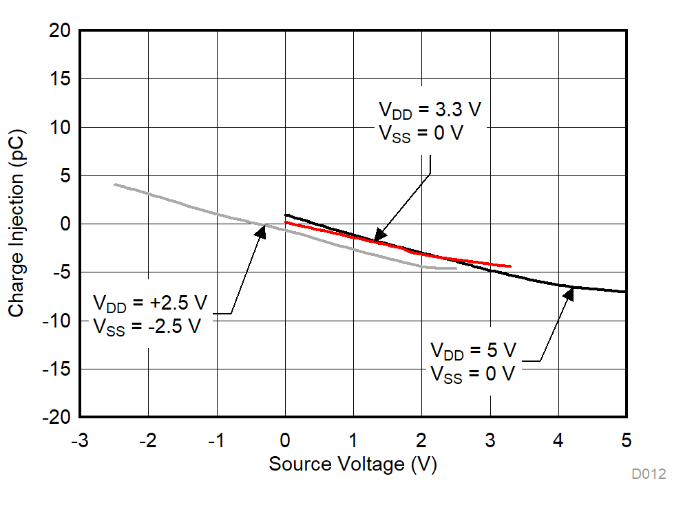
TA = -40°C to 125°C
Figure 6-12 Charge Injection vs Source Voltage
GUID-F4FD9980-CF66-4821-92F8-58534CD3E198-low.gif
TA = -40°C to +125°C
Figure 6-14 Xtalk and Off-Isolation vs Frequency