JAJSR31 august 2023 TMUX121
PRODUCTION DATA
8.4.1 Layout Guidelines
Place supply bypass capacitors as close to VDD pin as possible and avoid placing the bypass capacitors near the high speed traces.
Route the high-speed signals using a minimum of vias and corners which reduces signal reflections and impedance changes. When a via must be used, increase the clearance size around it to minimize its capacitance. Each via introduces discontinuities in the signal’s transmission line and increases the chance of picking up interference from the other layers of the board. Be careful when designing test points on twisted pair lines; through-hole pins are not recommended.
When it becomes necessary to turn 90°, use two 45° turns or an arc instead of making a single 90° turn. Doing this reduces reflections on the signal traces by minimizing impedance discontinuities. Avoid stubs on the high-speed signals because they cause signal reflections. Route all high-speed signal traces over continuous planes (VDD or GND) with no interruptions.
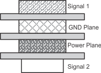
Due to high frequencies, a printed circuit board with at least four layers is recommended; two signal layers separated by a ground and power layer as shown in Figure 8-3.
 Figure 8-3 Four-Layer Board Stack-Up
The majority of signal traces must run on a single layer, preferably Signal 1. Immediately next to this layer must be the GND plane, which is solid with no cuts. Avoid running signal traces across a split in the ground or power plane. When running across split planes is unavoidable, sufficient decoupling must be used. Minimizing the number of signal vias reduces EMI by reducing inductance at high frequencies.
For high speed layout guidelines, refer to High-Speed Layout Guidelines application note.