JAJSGD8B October 2018 – Sept 2019 TMUX1574
PRODUCTION DATA.
- 1 特長
- 2 アプリケーション
- 3 概要
- 4 改訂履歴
- 5 概要 (続き)
- 6 Pin Configuration and Functions
- 7 Specifications
-
8 Parameter Measurement Information
- 8.1 On-Resistance
- 8.2 Off-Leakage Current
- 8.3 On-Leakage Current
- 8.4 IPOFF Leakage Current
- 8.5 Transition Time
- 8.6 tON (EN) and tOFF (EN) Time
- 8.7 tON (VDD) and tOFF (VDD) Time
- 8.8 Break-Before-Make Delay
- 8.9 Propagation Delay
- 8.10 Skew
- 8.11 Charge Injection
- 8.12 Capacitance
- 8.13 Off Isolation
- 8.14 Channel-to-Channel Crosstalk
- 8.15 Bandwidth
- 9 Detailed Description
- 10Application and Implementation
- 11Power Supply Recommendations
- 12Layout
- 13デバイスおよびドキュメントのサポート
- 14メカニカル、パッケージ、および注文情報
パッケージ・オプション
メカニカル・データ(パッケージ|ピン)
サーマルパッド・メカニカル・データ
発注情報
8.3 On-Leakage Current
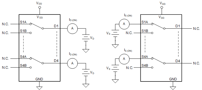
Source on-leakage current is defined as the leakage current flowing into or out of the source pin when the switch is on. This current is denoted by the symbol IS (ON).
Drain on-leakage current is defined as the leakage current flowing into or out of the drain pin when the switch is on. This current is denoted by the symbol ID (ON).
Either the source pin or drain pin is left floating during the measurement. Figure 29 shows the circuit used for measuring the on-leakage current, denoted by IS(ON) or ID(ON).
 Figure 29. On-Leakage Measurement Setup