JAJSO44A June 2023 – September 2024 TMUX582F-SEP
PRODUCTION DATA
- 1
- 1 特長
- 2 アプリケーション
- 3 概要
- 4 Pin Configuration and Functions
- 5 Specifications
-
6 Parameter Measurement Information
- 6.1 On-Resistance
- 6.2 Off-Leakage Current
- 6.3 On-Leakage Current
- 6.4 Input and Output Leakage Current Under Overvoltage Fault
- 6.5 Break-Before-Make Delay
- 6.6 Enable Delay Time
- 6.7 Transition Time
- 6.8 Fault Response Time
- 6.9 Fault Recovery Time
- 6.10 Fault Flag Response Time
- 6.11 Fault Flag Recovery Time
- 6.12 Charge Injection
- 6.13 Off Isolation
- 6.14 Crosstalk
- 6.15 Bandwidth
- 6.16 THD + Noise
- 7 Truth Table
- 8 Detailed Description
- 9 Application and Implementation
- 10Device and Documentation Support
- 11Revision History
- 12Mechanical, Packaging, and Orderable Information
パッケージ・オプション
デバイスごとのパッケージ図は、PDF版データシートをご参照ください。
メカニカル・データ(パッケージ|ピン)
- PW|20
サーマルパッド・メカニカル・データ
発注情報
4 Pin Configuration and Functions
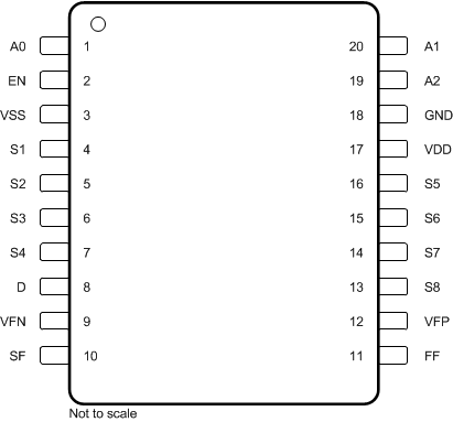
 Figure 4-1 PW Package, 20-Pin TSSOP (Top
View)
Figure 4-1 PW Package, 20-Pin TSSOP (Top
View)Table 4-1 Pin Functions: TMUX582F-SEP
| PIN | TYPE(1) | DESCRIPTION | |
|---|---|---|---|
| NAME | NO. | ||
| A0 | 1 | I | Logic control input address 0 (A0). The pin has a weak internal pull-down. This pin can also be used together with the specific fault pin (SF) to indicate which input is under fault. |
| EN | 2 | I | Active high digital enable (EN) pin. The pin has a weak internal pull-down. The device is disabled and all switches become high impedance when the pin is low. When the pin is high, the Ax logic inputs determine individual switch states. |
| VSS | 3 | P | Negative power supply. This pin must be tied to GND. |
| S1 | 4 | I/O | Overvoltage protected source pin 1. Can be an input or output. |
| S2 | 5 | I/O | Overvoltage protected source pin 2. Can be an input or output. |
| S3 | 6 | I/O | Overvoltage protected source pin 3. Can be an input or output. |
| S4 | 7 | I/O | Overvoltage protected source pin 4. Can be an input or output. |
| D | 8 | I/O | Drain pin. Can be an input or output. The drain pin is not overvoltage protected and shall remain within the recommended operating range. |
| VFN | 9 | P | Negative fault voltage supply that determines the overvoltage protection triggering threshold on the negative side. This pin must be tied to GND. |
| SF | 10 | O | Specific fault flag. This pin is an open drain output and is asserted low when overvoltage condition is detected on a specific pin, depending on the state of A0, A1, and A2 , as shown in Table 7-1. Connect this pin to an external supply (1.8V to 5.5V) through a 1kΩ pull-up resistor. |
| FF | 11 | O | General fault flag. This pin is an open drain output and is asserted low when overvoltage condition is detected on any of the source (Sx) input pins. Connect this pin to an external supply (1.8V to 5.5V) through a 1kΩ pull-up resistor. |
| VFP | 12 | P | Positive fault voltage supply that determines the overvoltage protection triggering threshold on the positive side. Connect to VDD if the triggering threshold is to be the same as the device's positive supply. For reliable operation, connect a decoupling capacitor ranging from 0.1µF to 10µF between VFP and GND. |
| S8 | 13 | I/O | Overvoltage protected source pin 8. Can be an input or output. |
| S7 | 14 | I/O | Overvoltage protected source pin 7. Can be an input or output. |
| S6 | 15 | I/O | Overvoltage protected source pin 6. Can be an input or output. |
| S5 | 16 | I/O | Overvoltage protected source pin 5. Can be an input or output. |
| VDD | 17 | P | Positive power supply. This pin is the most positive power-supply potential. For reliable operation, connect a decoupling capacitor ranging from 0.1µF to 10µF between VDD and GND. |
| GND | 18 | P | Ground (0V) reference |
| A2 | 19 | I | Logic control input address 2 (A2). The pin has a weak internal pull-down. This pin can also be used together with the specific fault pin (SF) to indicate which input is under fault. |
| A1 | 20 | I | Logic control input address 1 (A1). The pin has a weak internal pull-down. This pin can also be used together with the specific fault pin (SF) to indicate which input is under fault. |
(1) I = input, O = output, I/O = input and output, P = power