JAJSES2A February 2018 – September 2018 TMUX6104
PRODUCTION DATA.
- 1 特長
- 2 アプリケーション
- 3 概要
- 4 改訂履歴
- 5 Pin Configuration and Functions
-
6 Specifications
- 6.1 Absolute Maximum Ratings
- 6.2 ESD Ratings
- 6.3 Thermal Information
- 6.4 Recommended Operating Conditions
- 6.5 Electrical Characteristics (Dual Supplies: ±15 V)
- 6.6 Switching Characteristics (Dual Supplies: ±15 V)
- 6.7 Electrical Characteristics (Single Supply: 12 V)
- 6.8 Switching Characteristics (Single Supply: 12 V)
- 6.9 Typical Characteristics
- 7 Parameter Measurement Information
-
8 Detailed Description
- 8.1
Overview
- 8.1.1 On-Resistance
- 8.1.2 Off-Leakage Current
- 8.1.3 On-Leakage Current
- 8.1.4 Transition Time
- 8.1.5 Break-Before-Make Delay
- 8.1.6 Turn-On and Turn-Off Time
- 8.1.7 Charge Injection
- 8.1.8 Off Isolation
- 8.1.9 Channel-to-Channel Crosstalk
- 8.1.10 Bandwidth
- 8.1.11 THD + Noise
- 8.1.12 AC Power Supply Rejection Ratio (AC PSRR)
- 8.2 Functional Block Diagram
- 8.3 Feature Description
- 8.4 Device Functional Modes
- 8.1
Overview
- 9 Application and Implementation
- 10Power Supply Recommendations
- 11Layout
- 12デバイスおよびドキュメントのサポート
- 13メカニカル、パッケージ、および注文情報
8.3.2 Ultralow Charge Injection
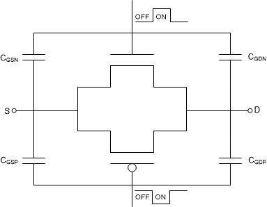
The TMUX6104 is implemented with simple transmission gate topology, as shown in Figure 30. Any mismatch in the stray capacitance associated with the NMOS and PMOS causes an output level change whenever the switch is opened or closed.
 Figure 30. Transmission Gate Topology
 The TMUX6119 utilizes special charge-injection cancellation circuitry that reduces the source (Sx) to drain (D) charge injection to as low as –0.35 pC at VS = 0 V, and –0.41 pC in the full signal range, as shown in Figure 31.
 Figure 31. Source-to-Drain Charge Injection vs Source Voltage
 The drain (D)-to-source (Sx) charge injection becomes important when the device is used as a demultiplexer (demux), where the drain (D) becomes the input and the source (Sx) becomes the output. Figure 32 shows the drain-to-source charge injection across the full signal range.
 Figure 32. Drain-to-Source Charge Injection vs Drain Voltage