JAJSG83A September 2018 – December 2018 TMUX6119
PRODUCTION DATA.
- 1 特長
- 2 アプリケーション
- 3 概要
- 4 改訂履歴
- 5 Pin Configuration and Functions
-
6 Specifications
- 6.1 Absolute Maximum Ratings
- 6.2 ESD Ratings
- 6.3 Thermal Information
- 6.4 Recommended Operating Conditions
- 6.5 Electrical Characteristics (Dual Supplies: ±15 V)
- 6.6 Switching Characteristics (Dual Supplies: ±15 V)
- 6.7 Electrical Characteristics (Single Supply: 12 V)
- 6.8 Switching Characteristics (Single Supply: 12 V)
- 6.9 Typical Characteristics
- 7 Parameter Measurement Information
-
8 Detailed Description
- 8.1
Overview
- 8.1.1 On-Resistance
- 8.1.2 Off-Leakage Current
- 8.1.3 On-Leakage Current
- 8.1.4 Transition Time
- 8.1.5 Break-Before-Make Delay
- 8.1.6 Enable Turn-On and Enable Turn-Off Time
- 8.1.7 Charge Injection
- 8.1.8 Off Isolation
- 8.1.9 Channel-to-Channel Crosstalk
- 8.1.10 Bandwidth
- 8.1.11 THD + Noise
- 8.1.12 AC Power Supply Rejection Ratio (AC PSRR)
- 8.2 Functional Block Diagram
- 8.3 Feature Description
- 8.4 Device Functional Modes
- 8.1
Overview
- 9 Application and Implementation
- 10Power Supply Recommendations
- 11Layout
- 12デバイスおよびドキュメントのサポート
- 13メカニカル、パッケージ、および注文情報
8.1.9 Channel-to-Channel Crosstalk
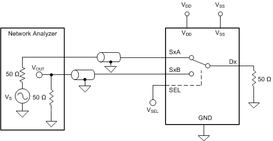
Channel-to-channel crosstalk is defined as the voltage at the source pin (SA or SB) of an off-channel, when a 1-VRMS signal is applied at the source pin of an on-channel. Figure 26 shows the setup used to measure, and Equation 3 is the equation used to compute, channel-to-channel crosstalk.
 Figure 26. Channel-to-Channel Crosstalk Measurement Setup
 Equation 3. 
