JAJSM45 June   2021 TMUX646

PRODUCTION DATA  

  1. 特長
  2. アプリケーション
  3. 概要
  4. Revision History
  5. Pin Configuration and Functions
  6. Specifications
    1. 6.1 Absolute Maximum Ratings
    2. 6.2 ESD Ratings
    3. 6.3 Recommended Operating Conditions
    4. 6.4 Thermal Information
    5. 6.5 Electrical Characteristics
    6. 6.6 Typical Characteristics
  7. Parameter Measurement Information
  8. Detailed Description
    1. 8.1 Overview
    2. 8.2 Functional Block Diagram
    3. 8.3 Feature Description
      1. 8.3.1 1.2-V Logic Compatible Inputs
      2. 8.3.2 Bidirectional Operation
      3. 8.3.3 Powered-Off Protection
      4. 8.3.4 Low Power Disable Mode
    4. 8.4 Device Functional Modes
      1. 8.4.1 Pin Functions
      2. 8.4.2 Low Power Disable Mode
      3. 8.4.3 Switch Enabled Mode
  9. Application and Implementation
    1. 9.1 Application Information
    2. 9.2 Typical Application
      1. 9.2.1 Design Requirements
      2. 9.2.2 Detailed Design Procedure
        1. 9.2.2.1 MIPI D-PHY Application
        2. 9.2.2.2 MIPI C-PHY Application
      3. 9.2.3 Application Curves
  10. 10Power Supply Recommendations
  11. 11Layout
    1. 11.1 Layout Guidelines
    2. 11.2 Layout Example
  12. 12Device and Documentation Support
    1. 12.1 Documentation Support
      1. 12.1.1 Related Documentation
    2. 12.2 Receiving Notification of Documentation Updates
    3. 12.3 サポート・リソース
    4. 12.4 Trademarks
    5. 12.5 Electrostatic Discharge Caution
    6. 12.6 Glossary
  13. 13Mechanical, Packaging, and Orderable Information

パッケージ・オプション

メカニカル・データ(パッケージ|ピン)
サーマルパッド・メカニカル・データ
発注情報

MIPI D-PHY Application

The clock and data lanes can be interchanged as necessary to facilitate the best layout possible for the application. In addition, the signal lines of the TMUX646 are routed single ended on the chip die. This makes the device suitable for differential and single-ended high-speed systems. This also allows the positive and negative lines to be interchanged as necessary to facilitate the best layout possible for the application.

D-PHY application includes a differential clock and 4 differential data lanes. All the channels of the device perform similar and the clock or data signals can be interchanged as necessary to facilitate the best layout possible for the application.
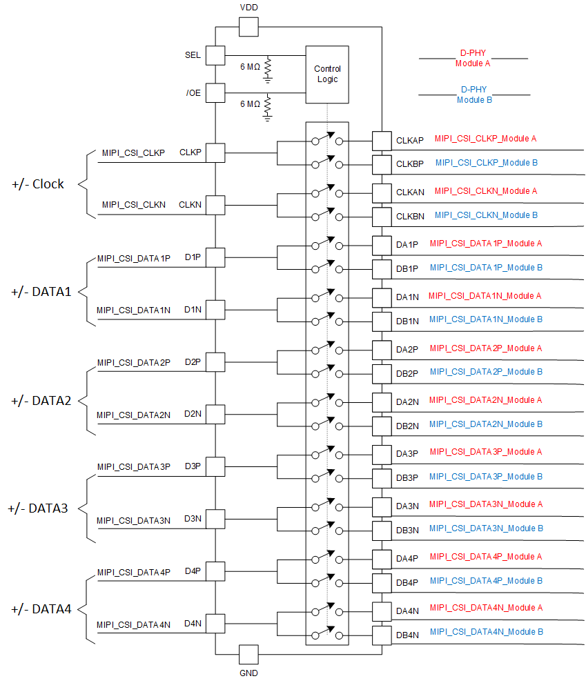
GUID-7892BDBF-D41B-4FFC-BD34-C453216E26AD-low.gif Figure 9-3 MIPI D-PHY Example Pinout