JAJSOU4C November   2011  – June 2022 TPA2015D1

PRODUCTION DATA  

  1. 特長
  2. アプリケーション
  3. 説明
  4. Revision History
  5. Device Comparison Table
  6. Pin Configuration and Functions
  7. Specifications
    1. 7.1 Absolute Maximum Ratings
    2. 7.2 ESD Ratings
    3. 7.3 Recommended Operating Conditions
    4. 7.4 Thermal Information
    5. 7.5 Electrical Characteristics
    6. 7.6 Operating Characteristics
    7. 7.7 Typical Characteristics
  8. Parameter Measurement Information
  9. Detailed Description
    1. 9.1 Overview
    2. 9.2 Functional Block Diagram
    3. 9.3 Feature Description
      1. 9.3.1 SpeakerGuard™ Theory of Operation
        1. 9.3.1.1 SpeakerGuard™ With Varying Input Levels
        2. 9.3.1.2 Battery Tracking SpeakerGuard™
      2. 9.3.2 Fully Differential Class-D Amplifier
        1. 9.3.2.1 Advantages of Fully Differential Amplifiers
        2. 9.3.2.2 Improved Class-D Efficiency
      3. 9.3.3 Adaptive Boost Converter
        1. 9.3.3.1 Boost Converter Overvoltage Protection
      4. 9.3.4 Operation With DACs and CODECs
      5. 9.3.5 Filter Free Operation and Ferrite Bead Filters
      6. 9.3.6 Speaker Load Limitation
      7. 9.3.7 Fixed Gain Setting
    4. 9.4 Device Functional Modes
      1. 9.4.1 Shutdown Mode
      2. 9.4.2 Battery Tracking SpeakerGuard™ Operation
  10. 10Application and Implementation
    1. 10.1 Application Information
    2. 10.2 Typical Applications
      1. 10.2.1 TPA2015D1 With Differential Input Signals
        1. 10.2.1.1 Design Requirements
        2. 10.2.1.2 Detailed Design Procedure
          1. 10.2.1.2.1 Boost Converter Inductor Selection
            1. 10.2.1.2.1.1 Inductor Equations
          2. 10.2.1.2.2 Boost Converter Capacitor Selection
          3. 10.2.1.2.3 Components Location and Selection
            1. 10.2.1.2.3.1 Decoupling Capacitors
            2. 10.2.1.2.3.2 Input Capacitors
        3. 10.2.1.3 Application Curves
      2. 10.2.2 TPA2015D1 with Single-Ended Input Signals
        1. 10.2.2.1 Design Requirements
        2. 10.2.2.2 Detailed Design Procedure
        3. 10.2.2.3 Application Curves
  11. 11Power Supply Recommendations
    1. 11.1 Power Supply Decoupling Capacitors
  12. 12Layout
    1. 12.1 Layout Guidelines
      1. 12.1.1 Component Placement
      2. 12.1.2 Trace Width
      3. 12.1.3 Pad Size
    2. 12.2 Layout Example
  13. 13Device and Documentation Support
    1. 13.1 Device Support
      1. 13.1.1 Device Nomenclature
        1. 13.1.1.1 TPA2015D1 Glossary
        2. 13.1.1.2 Boost Terms
    2. 13.2 Community Resources
    3. 13.3 Trademarks
  14. 14Mechanical, Packaging, and Orderable Information
    1. 14.1 Package Option Addendum
      1. 14.1.1 Packaging Information
      2. 14.1.2 Tape and Reel Information

パッケージ・オプション

メカニカル・データ(パッケージ|ピン)
サーマルパッド・メカニカル・データ
発注情報

Parameter Measurement Information

All parameters are measured according to the conditions described in the Section 7 section.

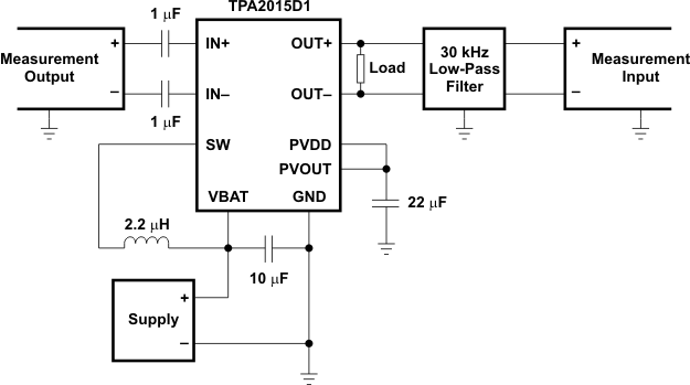
Figure 8-1 shows the setup used to test the device's typical characteristics.
GUID-8E11B9E4-05D4-4A37-8291-7C7B421BB335-low.gif
The 1 µF input capacitors (CI) were shorted for input common-mode voltage measurements.
A 33 μH inductor was placed in series with the load resistor to emulate a small speaker for efficiency measurements.
The 30 kHz low-pass filter is required even if the analyzer has an internal low-pass filter. An R-C low pass filter (100 Ω, 47 nF) is used on each output for the data sheet graphs.
Figure 8-1 Test Setup for Typical Characteristics Graphs