JAJSOU4C November   2011  – June 2022 TPA2015D1

PRODUCTION DATA  

  1. 特長
  2. アプリケーション
  3. 説明
  4. Revision History
  5. Device Comparison Table
  6. Pin Configuration and Functions
  7. Specifications
    1. 7.1 Absolute Maximum Ratings
    2. 7.2 ESD Ratings
    3. 7.3 Recommended Operating Conditions
    4. 7.4 Thermal Information
    5. 7.5 Electrical Characteristics
    6. 7.6 Operating Characteristics
    7. 7.7 Typical Characteristics
  8. Parameter Measurement Information
  9. Detailed Description
    1. 9.1 Overview
    2. 9.2 Functional Block Diagram
    3. 9.3 Feature Description
      1. 9.3.1 SpeakerGuard™ Theory of Operation
        1. 9.3.1.1 SpeakerGuard™ With Varying Input Levels
        2. 9.3.1.2 Battery Tracking SpeakerGuard™
      2. 9.3.2 Fully Differential Class-D Amplifier
        1. 9.3.2.1 Advantages of Fully Differential Amplifiers
        2. 9.3.2.2 Improved Class-D Efficiency
      3. 9.3.3 Adaptive Boost Converter
        1. 9.3.3.1 Boost Converter Overvoltage Protection
      4. 9.3.4 Operation With DACs and CODECs
      5. 9.3.5 Filter Free Operation and Ferrite Bead Filters
      6. 9.3.6 Speaker Load Limitation
      7. 9.3.7 Fixed Gain Setting
    4. 9.4 Device Functional Modes
      1. 9.4.1 Shutdown Mode
      2. 9.4.2 Battery Tracking SpeakerGuard™ Operation
  10. 10Application and Implementation
    1. 10.1 Application Information
    2. 10.2 Typical Applications
      1. 10.2.1 TPA2015D1 With Differential Input Signals
        1. 10.2.1.1 Design Requirements
        2. 10.2.1.2 Detailed Design Procedure
          1. 10.2.1.2.1 Boost Converter Inductor Selection
            1. 10.2.1.2.1.1 Inductor Equations
          2. 10.2.1.2.2 Boost Converter Capacitor Selection
          3. 10.2.1.2.3 Components Location and Selection
            1. 10.2.1.2.3.1 Decoupling Capacitors
            2. 10.2.1.2.3.2 Input Capacitors
        3. 10.2.1.3 Application Curves
      2. 10.2.2 TPA2015D1 with Single-Ended Input Signals
        1. 10.2.2.1 Design Requirements
        2. 10.2.2.2 Detailed Design Procedure
        3. 10.2.2.3 Application Curves
  11. 11Power Supply Recommendations
    1. 11.1 Power Supply Decoupling Capacitors
  12. 12Layout
    1. 12.1 Layout Guidelines
      1. 12.1.1 Component Placement
      2. 12.1.2 Trace Width
      3. 12.1.3 Pad Size
    2. 12.2 Layout Example
  13. 13Device and Documentation Support
    1. 13.1 Device Support
      1. 13.1.1 Device Nomenclature
        1. 13.1.1.1 TPA2015D1 Glossary
        2. 13.1.1.2 Boost Terms
    2. 13.2 Community Resources
    3. 13.3 Trademarks
  14. 14Mechanical, Packaging, and Orderable Information
    1. 14.1 Package Option Addendum
      1. 14.1.1 Packaging Information
      2. 14.1.2 Tape and Reel Information

パッケージ・オプション

メカニカル・データ(パッケージ|ピン)
サーマルパッド・メカニカル・データ
発注情報

SpeakerGuard™ With Varying Input Levels

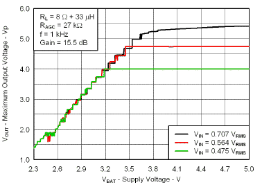
SpeakerGuard™ protects speakers by decreasing gain during large output transients. Figure 9-2 shows the maximum output voltage at different input voltage levels. The load is 8 Ω and the gain is 15.5 dB (6 V/V).
GUID-D970A215-5241-4F47-BF8A-22D643FE60DB-low.gif
Figure 9-2 Maximum Output Voltage vs Supply Voltage

A 0.707 VRMS sine-wave input signal forces the output voltage to 4.242 VRMS, or 6.0 VPEAK. Above 3.9 V supply, the boost converter voltage sags due to high output current, resulting in a peak Class-D output voltage of about 5.4 V. As the supply voltage decreases below 3.9 V, the limiter level decreases. This causes the gain to decrease, and the peak Class-D output voltage lowers.

With a 0.564 VRMS input signal, the peak Class-D output voltage is 4.78 V. When the supply voltage is above 3.45 V, the output voltage remains below the limiter level, and the gain stays at 15.5 dB. Once the supply drops below 3.45 V, the limiter level decreases below 4.78 V, and SpeakerGuard™ decreases the gain.

The same rationale applies to the 0.475 VRMS input signal. Although the supply voltage may be below the inflection point, audio gain does not decrease until the Class-D output voltage is above the limiter level.