SLOS649B March 2010 – May 2016 TPA2026D2
PRODUCTION DATA.
- 1 Features
- 2 Applications
- 3 Description
- 4 Revision History
- 5 Device Comparison Table
- 6 Pin Configuration and Functions
- 7 Specifications
- 8 Parameter Measurement Information
- 9 Detailed Description
- 10Application and Implementation
- 11Power Supply Recommendations
- 12Layout
- 13Device and Documentation Support
- 14Mechanical, Packaging, and Orderable Information
9 Detailed Description
9.1 Overview
The TPA2026D2 is a stereo Class-D audio power amplifier capable of driving 750 mW/Ch into 8-Ω load at 3.6 V and 3.2 W/Ch into 4-Ω load at 5 V. The device features independent software shutdown controls for each channel and also provides thermal and short-circuit protection. In addition to these features, a fast start-up time and small package size make the TPA2026D2 an ideal choice for cellular handsets, PDAs, and other portable applications.
9.2 Functional Block Diagram
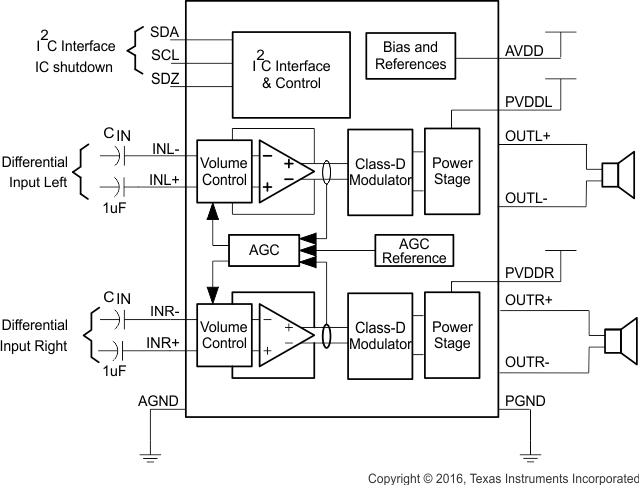
9.3 Feature Description
9.3.1 Automatic Gain Control
The Automatic Gain Control (AGC) feature provides continuous automatic gain adjustment to the amplifier through an internal PGA. This feature enhances the perceived audio loudness and at the same time prevents speaker damage from occurring (Limiter function).
The AGC function attempts to maintain the audio signal gain as selected by the user through the Fixed Gain, Limiter Level, and Compression Ratio variables. Other advanced features included are Maximum Gain and Noise Gate Threshold. Table 2 describes the function of each variable in the AGC function.
Table 2. TPA2026D2 AGC Variable Descriptions
| VARIABLE | DESCRIPTION |
|---|---|
| Maximum Gain | The gain at the lower end of the compression region. |
| Fixed Gain | The normal gain of the device when the AGC is inactive. |
| The fixed gain is also the initial gain when the device comes out of shutdown mode or when the AGC is disabled. | |
| Limiter Level | The value that sets the maximum allowed output amplitude. |
| Compression Ratio | The relation between input and output voltage. |
| Noise Gate Threshold | Below this value, the AGC holds the gain to prevent breathing effects. |
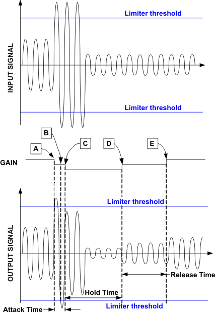
| Attack Time | The minimum time between two gain decrements. |
| Release Time | The minimum time between two gain increments. |
| Hold Time | The time it takes for the very first gain increment after the input signal amplitude decreases. |
The AGC works by detecting the audio input envelope. The gain changes depending on the amplitude, the limiter level, the compression ratio, and the attack and release time. The gain changes constantly as the audio signal increases and/or decreases to create the compression effect. The gain step size for the AGC is 0.5 dB. If the audio signal has near-constant amplitude, the gain does not change. Figure 32 shows how the AGC works.
Because the number of gain steps is limited the compression region is limited as well. Figure 33 shows how the gain changes versus the input signal amplitude in the compression region.
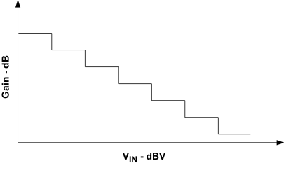 Figure 33. Input Signal Voltage vs Gain
Thus the AGC performs a mapping of the input signal versus the output signal amplitude. This mapping can be modified according to the variables from Table 2.
The following graphs and explanations show the effect of each variable to the AGC independently and which considerations should be taken when choosing values.
9.3.1.1 Fixed Gain
The fixed gain determines the initial gain of the AGC. Set the gain using the following variables:
- Set the fixed gain to be equal to the gain when the AGC is disabled.
- Set the fixed gain to maximize SNR.
- Set the fixed gain such that it will not overdrive the speaker.
Figure 34 shows how the fixed gain influences the input signal amplitude versus the output signal amplitude state diagram. The dotted 1:1 line is displayed for reference. The 1:1 line means that for a 1-dB increase in the input signal, the output increases by 1 dB.
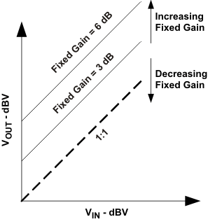 Figure 34. Output Signal vs Input Signal State Diagram Showing Different Fixed Gain Configurations
If the Compression function is enabled, the Fixed Gain is adjustable from –28 dB to 30 dB. If the Compression function is disabled, the Fixed gain is adjustable from 0 dB to 30 dB.
9.3.1.2 Limiter Level
The Limiter level sets the maximum amplitude allowed at the output of the amplifier. The limiter should be set with the following constraints in mind:
- Below or at the maximum power rating of the speaker
- Below the minimum supply voltage in order to avoid clipping
Figure 35 shows how the limiter level influences the input signal amplitude versus the output signal amplitude state diagram.
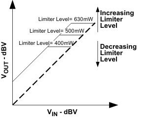 Figure 35. Output Signal vs Input Signal State Diagram Showing Different Limiter Level Configurations
The limiter level and the fixed gain influence each other. If the fixed gain is set high, the AGC has a large limiter range. The fixed gain is set low, the AGC has a short limiter range. Figure 36 illustrates the two examples:
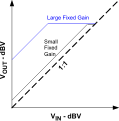 Figure 36. Output Signal vs Input Signal State Diagram Showing Same Limiter Level Configurations With Different Fixed Gain Configurations
9.3.1.3 Compression Ratio
The compression ratio sets the relation between input and output signal outside the limiter level region. The compression ratio compresses the dynamic range of the audio. For example if the audio source has a dynamic range of 60 dB and compression ratio of 2:1 is selected, then the output has a dynamic range of 30 dB. Most small form factor speakers have small dynamic range. Compression ratio allows audio with large dynamic range to fit into a speaker with small dynamic range.
The compression ratio also increases the loudness of the audio without increasing the peak voltage. The higher the compression ratio, the louder the perceived audio.
For example:
- A compression ratio of 4:1 is selected (meaning that a 4-dB change in the input signal results in a 1-dB signal change at the output)
- A fixed gain of 0 dB is selected and the maximum audio level is at 0 dBV.
When the input signal decreases to –32 dBV, the amplifier increases the gain to 24 dB in order to achieve an output of –8 dBV. The output signal amplitude equation is:

In this example:

The gain change equation is:


Consider the following when setting the compression ratio:
- Dynamic range of the speaker
- Fixed gain level
- Limiter Level
- Audio Loudness vs Output Dynamic Range
Figure 37 shows different settings for dynamic range and different fixed gain selected but no limiter level.
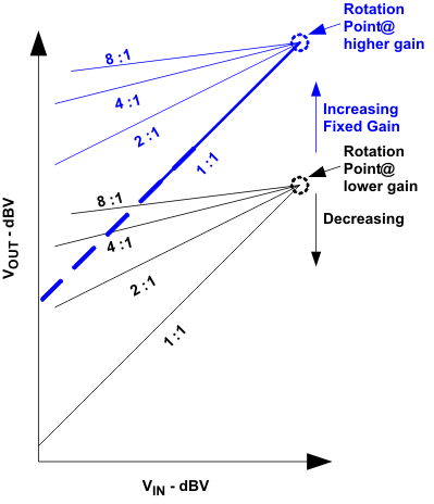 Figure 37. Output Signal vs Input Signal State Diagram Showing Different Compression Ratio Configurations With Different Fixed Gain Configurations
The rotation point is always at VIN = 10 dBV. The rotation point is not located at the intersection of the limiter region and the compression region. By changing the fixed gain the rotation point will move in the y-axis direction only, as shown in the previous graph.
9.3.1.4 Interaction Between Compression Ratio and Limiter Range
The compression ratio can be limited by the limiter range.
NOTE
The limiter range is selected by the limiter level and the fixed gain.
For a setting with large limiter range, the amount of gain steps in the AGC remaining to perform compression are limited. Figure 38 shows two examples, where the fixed gain was changed.
- Small limiter range yielding a large compression region (small fixed gain).
- Large limiter range yielding a small compression region (large fixed gain).
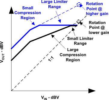 Figure 38. Output Signal vs Input Signal State Diagram Showing the Effects of the Limiter Range to the Compression Region
9.3.1.5 Noise Gate Threshold
The noise gate threshold prevents the AGC from changing the gain when there is no audio at the input of the amplifier. The noise gate threshold stops gain changes until the input signal is above the noise gate threshold. Select the noise gate threshold to be above the noise but below the minimum audio at the input of the amplifier signal. A filter is needed between delta-sigma CODEC/DAC and TPA2026D2 for effectiveness of the noise gate function. The filter eliminates the out-of-band noise from delta-sigma modulation and keeps the CODEC/DAC output noise lower than the noise gate threshold.
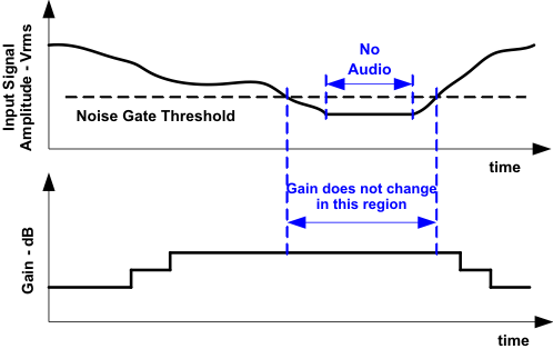 Figure 39. Time Diagram Showing the Relationship Between Input Signal Amplitude, Noise Gate Threshold, and Gain Versus Time
9.3.1.6 Maximum Gain
This variable limits the number of gain steps in the AGC. This feature is useful in order to accomplish a more advanced output signal versus input signal transfer characteristic.
For example, to prevent the gain from going above a certain value, reduce the maximum gain.
However, this variable will affect the limiter range and the compression region. If the maximum gain is decreased, the limiter range and/or compression region is reduced. Figure 40 illustrates the effects.
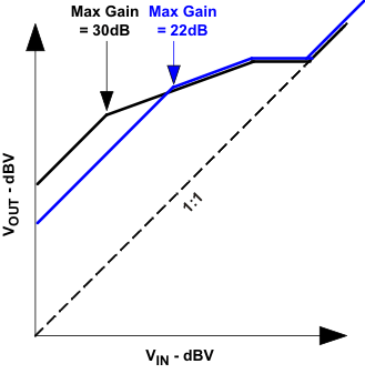 Figure 40. Output Signal vs Input Signal State Diagram Showing Different Maximum Gains
A particular application requiring maximum gain of 22 dB, for example. Thus, set the maximum gain at 22 dB. The amplifier gain never has a gain higher than 22 dB; however, this reduces the limiter range.
9.3.1.7 Attack, Release, and Hold Time
- The attack time is the minimum time between gain decreases.
- The release time is the minimum time between gain increases.
- The hold time is the minimum time between a gain decrease (attack) and a gain increase (release). The hold time can be deactivated. Hold time is only valid if greater than release time.
Successive gain decreases are never faster than the attack time. Successive gain increases are never faster than the release time.
All time variables (attack, release, and hold) start counting after each gain change performed by the AGC. The AGC is allowed to decrease the gain (attack) only after the attack time finishes. The AGC is allowed to increase the gain (release) only after the release time finishes counting. However, if the preceding gain change was an attack (gain increase) and the hold time is enabled and longer than the release time, then the gain is only increased after the hold time.
The hold time is only enabled after a gain decrease (attack). The hold time replaces the release time after a gain decrease (attack). If the gain needs to be increased further, then the release time is used. The release time is used instead of the hold time if the hold time is disabled.
The attack time must be at least 100 times shorter than the release and hold time. The hold time must be the same or greater than the release time. It is important to select reasonable values for those variables in order to prevent the gain from changing too often or too slow.
Figure 41 illustrates the relationship between the three time variables.
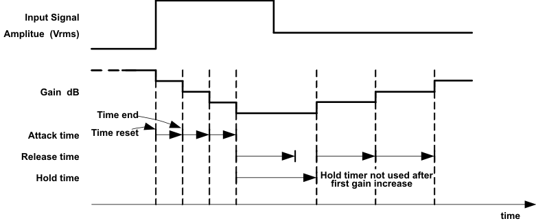 Figure 41. Time Diagram Showing the Relation Between the Attack, Release, and Hold Time vs Input Signal Amplitude and Gain
Figure 42 shows a state diagram of the input signal amplitude versus the output signal amplitude and a summary of how the variables from Table 2 described in the preceding pages affect them.
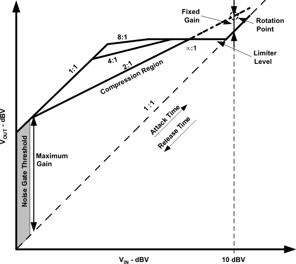 Figure 42. Output Signal vs Input Signal State Diagram
9.3.2 Operation With DACS and CODECS
In using Class-D amplifiers with CODECs and DACs, sometimes there is an increase in the output noise floor from the audio amplifier. This occurs when output frequencies of the CODEC/DAC mix with the Class-D switching frequency and create sum or difference components in the audio band. The noise increase can be solved by placing an RC low-pass filter between the CODEC/DAC and audio amplifier. The filter reduces high frequencies that cause the problem and allows proper performance.
If driving the TPA2016D2 input with 4th-order or higher ΔΣ DACs or CODECs, add an RC low-pass filter at each of the audio inputs (IN+ and IN–) of the TPA2016D2 to ensure best performance. The recommended resistor value is 100 Ω and the capacitor value of 47 nF.
9.3.3 Short-Circuit Auto-Recovery
When a short-circuit event happens, the TPA2026D2 goes to low duty cycle mode and tries to reactivate itself every 110 µs. This auto-recovery continues until the short-circuit event stops. This feature can protect the device without affecting the device's long-term reliability. FAULT bit (register 1, bit 3) still requires a write to clear.
9.3.4 Filter-Free Operation and Ferrite Bead Filters
A ferrite bead filter can often be used if the design is failing radiated emissions without an LC filter and the frequency-sensitive circuit is greater than 1 MHz. This filter functions well for circuits that just have to pass FCC and CE because FCC and CE only test radiated emissions greater than 30 MHz. When choosing a ferrite bead, choose one with high impedance at high frequencies, and low impedance at low frequencies. In addition, select a ferrite bead with adequate current rating to prevent distortion of the output signal.
Use an LC output filter if there are low frequency (< 1 MHz) EMI-sensitive circuits or there are long leads from amplifier to speaker. Figure 43 shows typical ferrite bead and LC output filters.
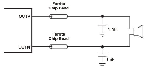 Figure 43. Typical Ferrite Bead Filter (Chip Bead Example: TDK: MPZ1608S221A)
9.4 Device Functional Modes
9.4.1 TPA2026D2 AGC Operation
The TPA2026D2 is controlled by the I2C interface. The correct start-up sequence is:
- Apply the supply voltage to the AVDD and PVDD (L, R) pins.
- Apply a voltage above VIH to the SDZ pin. The TPA2026D2 powers up the I2C interface and the control logic. By default, the device is in active mode (SWS = 0). After 5 ms the amplifier enables the class-D output stage and become fully operational.
9.4.1.1 AGC Start-Up Condition
The amplifier gain at start-up depends on the following conditions:
- Start-up from hardware reset (EN from 0 to 1): The amplifier starts up immediately at default fixed gain. AGC starts controlling gain once the input audio signal exceeds noise gate threshold.
- Start-up from software shutdown (SWS from 1 to 0): The amplifier starts up immediately at the latest fixed gain during software shutdown, regardless the attack or release time. For example:
- Audio is playing at fixed gain 6 dB
- Devices goes to software shutdown (SWS = 1)
- Set fixed gain from 6 dB to 12 dB
- Remove software shutdown (SWS = 0)
- Amplifier starts up immediately at 12 dB
- During audio playback with AGC on, gain changes according to attack or release time. For example:
- Audio is playing at fixed gain 6 dB and 1:1 compression ratio
- Set fixed gain from 6 dB to 12 dB, at release time 500 ms / 6 dB
- Amplifier takes 500 ms to ramp from 6 dB to 12 dB
- When SPKR_EN_R = 0, SPKR_EN_L = 0 and SWS = 0, the amplifier is set at fixed gain. The amplifier will start up at fixed gain when either SPKR_EN_R and SPKR_EN_L transitions from 0 to 1.
CAUTION
Do not interrupt the start-up sequence after changing SDZ from VIL to VIH.
Do not interrupt the start-up sequence after changing SWS from 1 to 0.
The default conditions of TPA2026D2 allows audio playback without I2C control. Refer to Table 5 for the entire default conditions.
There are several options to disable the amplifier:
- Write SPK_EN_R = 0 and SPK_EN_L = 0 to the register (0x01, 6 and 0x01, 7). This write disables each speaker amplifier, but leaves all other circuits operating.
- Write SWS = 1 to the register (0x01, 5). This action disables most of the amplifier functions.
- Apply VIL to SDZ. This action shuts down all the circuits and has very low quiescent current consumption. This action resets the registers to its default values.
CAUTION
Do not interrupt the shutdown sequence after changing SDZ from VIH to VIL.
Do not interrupt the shutdown sequence after changing SWS from 0 to 1.
9.4.2 TPA2026D2 AGC Recommended Settings
Table 3. Recommended AGC Settings for Different Types of Audio Source (VDD = 3.6 V)
| AUDIO SOURCE |
COMPRESSION RATIO |
ATTACK TIME (ms/6 dB) |
RELEASE TIME (ms/6 dB) |
HOLD TIME (ms) |
FIXED GAIN (dB) |
LIMITER LEVEL (dBV) |
|---|---|---|---|---|---|---|
| Pop Music | 4:1 | 1.28 to 3.84 | 986 to 1640 | 137 | 6 | 7.5 |
| Classical | 2:1 | 2.56 | 1150 | 137 | 6 | 8 |
| Jazz | 2:1 | 5.12 to 10.2 | 3288 | — | 6 | 8 |
| Rap/Hip Hop | 4:1 | 1.28 to 3.84 | 1640 | — | 6 | 7.5 |
| Rock | 2:1 | 3.84 | 4110 | — | 6 | 8 |
| Voice/News | 4:1 | 2.56 | 1640 | — | 6 | 8.5 |
9.5 Programming
9.5.1 General I2C Operation
The I2C bus employs two signals, SDA (data) and SCL (clock), to communicate between integrated circuits in a system. The bus transfers data serially one bit at a time. The address and data 8-bit bytes are transferred most significant bit (MSB) first. In addition, each byte transferred on the bus is acknowledged by the receiving device with an acknowledge bit. Each transfer operation begins with the master device driving a start condition on the bus and ends with the master device driving a stop condition on the bus. The bus uses transitions on the data terminal (SDA) while the clock is at logic high to indicate start and stop conditions. A high-to-low transition on SDA indicates a start and a low-to-high transition indicates a stop. Normal data-bit transitions must occur within the low time of the clock period. Figure 44 shows a typical sequence. The master generates the 7-bit slave address and the read/write (R/W) bit to open communication with another device, and then waits for an acknowledge condition. The TPA2026D2 holds SDA low during the acknowledge clock period to indicate acknowledgment. When this acknowledgment occurs, the master transmits the next byte of the sequence. Each device is addressed by a unique 7-bit slave address plus R/W bit (1 byte). All compatible devices share the same signals through a bidirectional bus using a wired-AND connection.
An external pullup resistor must be used for the SDA and SCL signals to set the logic high level for the bus. When the bus level is 5 V, use pullup resistors between 1 kΩ and 2 kΩ.
 Figure 44. Typical I2C Sequence
There is no limit on the number of bytes that can be transmitted between start and stop conditions. When the last word transfers, the master generates a stop condition to release the bus. A generic data transfer sequence is shown in Figure 44.
9.5.2 Single and Multiple-Byte Transfers
The serial control interface supports both single-byte and multi-byte read/write operations for all registers.
During multiple-byte read operations, the TPA2026D2 responds with data, one byte at a time, starting at the register assigned, as long as the master device continues to respond with acknowledgments.
The TPA2026D2 supports sequential I2C addressing. For write transactions, if a register is issued followed by data for that register and all the remaining registers that follow, a sequential I2C write transaction has occurred. For I2C sequential write transactions, the register issued then serves as the starting point, and the amount of data subsequently transmitted, before a stop or start is transmitted, determines the number of registers written.
9.5.3 Single-Byte Write
As Figure 45 shows, a single-byte data write transfer begins with the master device transmitting a start condition followed by the I2C device address and the read/write bit. The read/write bit determines the direction of the data transfer. For a write data transfer, the read/write bit must be set to 0. After receiving the correct I2C device address and the read/write bit, the TPA2026D2 responds with an acknowledge bit. Next, the master transmits the register byte corresponding to the TPA2026D2 internal memory address being accessed. After receiving the register byte, the TPA2026D2 again responds with an acknowledge bit. Next, the master device transmits the data byte to be written to the memory address being accessed. After receiving the register byte, the TPA2026D2 again responds with an acknowledge bit. Finally, the master device transmits a stop condition to complete the single-byte data write transfer.
 Figure 45. Single-Byte Write Transfer
9.5.4 Multiple-Byte Write and Incremental Multiple-Byte Write
A multiple-byte data write transfer is identical to a single-byte data write transfer except that multiple data bytes are transmitted by the master device to the TPA2026D2 as shown in Figure 46. After receiving each data byte, the TPA2026D2 responds with an acknowledge bit.
 Figure 46. Multiple-Byte Write Transfer
9.5.5 Single-Byte Read
As Figure 47 shows, a single-byte data read transfer begins with the master device transmitting a start condition followed by the I2C device address and the read/write bit. For the data read transfer, both a write followed by a read are actually executed. Initially, a write is executed to transfer the address byte of the internal memory address to be read. As a result, the read/write bit is set to a 0.
After receiving the TPA2026D2 address and the read/write bit, the TPA2026D2 responds with an acknowledge bit. The master then sends the internal memory address byte, after which the TPA2026D2 issues an acknowledge bit. The master device transmits another start condition followed by the TPA2026D2 address and the read/write bit again. This time the read/write bit is set to 1, indicating a read transfer. Next, the TPA2026D2 transmits the data byte from the memory address being read. After receiving the data byte, the master device transmits a not-acknowledge followed by a stop condition to complete the single-byte data read transfer.
 Figure 47. Single-Byte Read Transfer
9.5.6 Multiple-Byte Read
A multiple-byte data read transfer is identical to a single-byte data read transfer except that multiple data bytes are transmitted by the TPA2026D2 to the master device as shown in Figure 48. With the exception of the last data byte, the master device responds with an acknowledge bit after receiving each data byte.
 Figure 48. Multiple-Byte Read Transfer
9.6 Register Maps
Table 4. TPA2026D2 Register Map
| REGISTER | BIT7 | BIT6 | BIT5 | BIT4 | BIT3 | BIT2 | BIT1 | BIT0 |
|---|---|---|---|---|---|---|---|---|
| 1 | SPK_EN_R | SPL_EN_L | SWS | FAULT_R | FAULT_L | Thermal | 1 | NG_EN |
| 2 | 0 | 0 | ATK_time [5] | ATK_time [4] | ATK_time [3] | ATK_time [2] | ATK_time [1] | ATK_time [0] |
| 3 | 0 | 0 | REL_time [5] | REL_time [4] | REL_time [3] | REL_time [2] | REL_time [1] | REL_time [0] |
| 4 | 0 | 0 | Hold_time [5] | Hold_time [4] | Hold_tme [3] | Hold_time [2] | Hold_time [1] | Hold_time [0] |
| 5 | 0 | 0 | FixedGain [5] | FixedGain [4] | FixedGain [3] | FixedGain [2] | FixedGain [1] | FixedGain [0] |
| 6 | Output Limiter Disable | NoiseGate Threshold [1] | NoiseGate Threshold [2] | Output Limiter Level [4] | Output Limiter Level [3] | Output Limiter Level [2] | Output Limiter Level [1] | Output Limiter Level [0] |
| 7 | Max Gain [3] | Max Gain [2] | Max Gain [1] | Max Gain [0] | 0 | 0 | Compression Ratio [1] | Compression Ratio [0] |
The default register map values are given in Table 5.
Table 5. TPA2026D2 Default Register Values
| REGISTER | 0x01 | 0x02 | 0x03 | 0x04 | 0x05 | 0x06 | 0x07 |
|---|---|---|---|---|---|---|---|
| Default | C3h | 05h | 0Bh | 00h | 06h | 3Ah | C2h |
Any register above address 0x08 is reserved for testing and must not be written to because it may change the function of the device. If read, these bits may assume any value.
Some of the default values can be reprogrammed through the I2C interface and written to the EEPROM. This function is useful to speed up the turnon time of the device and minimizes the number of I2C writes. If this is required, contact your local TI representative.
The TPA2026D2 I2C address is 0xB0 (binary 10110000) for writing and 0xB1 (binary 10110001) for reading. If a different I2C address is required, contact your local TI representative. See General I2C Operation for more details.
The following tables show the details of the registers, the default values, and the values that can be programmed through the I2C interface.
9.6.1 IC Function Control (Address: 1)
Table 6. IC Function Control (Address: 1)
| SPK_EN_R: | Enable bit for the right-channel amplifier. Amplifier is active when bit is high. This function is gated by thermal and returns once the IC is below the threshold temperature. |
| SPK_EN_L: | Enable bit for the left-channel amplifier. Amplifier is active when bit is high. This function is gated by thermal and returns once the IC is below the threshold temperature |
| SWS: | Software shutdown control. The device is in software shutdown when the bit is 1 (control, bias and oscillator are inactive). When the bit is 0 the control, bias and oscillator are enabled. |
| FAULT_L: | This bit indicates that an over-current event has occurred on the left channel with a 1. This bit is cleared by writing a 0 to it. |
| FAULT_R: | This bit indicates that an over-current event has occurred on the right channel with a 1. This bit is cleared by writing a 0 to it. |
| Thermal: | This bit indicates a thermal shutdown that was initiated by the hardware with a 1. This bit is deglitched and latched, and can be cleared by writing a 0 to it. |
| NG_EN: | Enable bit for the Noise Gate function. This function is enabled when this bit is high. This function can only be enabled when the Compression ratio is not 1:1. |
9.6.2 AGC Attack Control (Address: 2)
Table 7. AGC Attack Control (Address: 2)
| ATK_time | These bits set the attack time for the AGC function. The attack time is the minimum time between gain decreases. |
9.6.3 AGC Release Control (Address: 3)
Table 8. AGC Release Control (Address: 3)
| REL_time | These bits set the release time for the AGC function. The release time is the minimum time between gain increases. |
9.6.4 AGC Hold Time Control (Address: 4)
Table 9. AGC Hold Time Control(Address: 4)
| Hold_time | These bits set the hold time for the AGC function. The hold time is the minimum time between a gain decrease (attack) and a gain increase (release). The hold time can be deactivated. |
9.6.5 AGC Fixed Gain Control (Address: 5)
Table 10. AGC Fixed Gain Control (Address: 5)
| REGISTER ADDRESS | I2C BIT | LABEL | DEFAULT | DESCRIPTION | |||
|---|---|---|---|---|---|---|---|
| 05 (05H) – AGC Fixed Gain Control | 7:6 | Unused | 00 | ||||
| 5:0 | Fixed Gain | 000110 (6 dB) | Sets the fixed gain of the amplifier: two's complement | ||||
| Gain | |||||||
| 100100 | –28 dB | ||||||
| 100101 | –27 dB | ||||||
| 100110 | –26 dB | ||||||
| (gain increases by 1 dB with every step) | |||||||
| 111101 | –3 dB | ||||||
| 111110 | –2 dB | ||||||
| 111111 | –1 dB | ||||||
| 000000 | 0 dB | ||||||
| 000001 | 1 dB | ||||||
| 000010 | 2 dB | ||||||
| 000011 | 3 dB | ||||||
| (gain increases by 1dB with every step) | |||||||
| 011100 | 28 dB | ||||||
| 011101 | 29 dB | ||||||
| 011110 | 30 dB | ||||||
| Fixed Gain | These bits are used to select the fixed gain of the amplifier. If compression is enabled, fixed gain is adjustable from –28 dB to 30 dB. If compression is disabled, fixed gain is adjustable from 0 dB to 30 dB. |
9.6.6 AGC Control (Address: 6)
Table 11. AGC Control (Address: 6)
| REGISTER ADDRESS | I2C BIT | LABEL | DEFAULT | DESCRIPTION | |||
|---|---|---|---|---|---|---|---|
| 06 (06H) – AGC Control | 7 | Output Limiter Disable | 0 (enable) | Disables the output limiter function. Can only be disabled when the AGC compression ratio is 1:1 (off) | |||
| 6:5 | NoiseGate Threshold | 01 (4 mVrms) | Select the threshold of the noise gate | ||||
| Threshold | |||||||
| 00 | 1 mVrms | ||||||
| 01 | 4 mVrms | ||||||
| 10 | 10 mVrms | ||||||
| 11 | 20 mVrms | ||||||
| 4:0 | Output Limiter Level | 11010 (6.5 dBV) | Selects the output limiter level | ||||
| Output Power (Wrms) | Peak Output Voltage (Vp) | dBV | |||||
| 00000 | 0.03 | 0.67 | –6.5 | ||||
| 00001 | 0.03 | 0.71 | –6 | ||||
| 00010 | 0.04 | 0.75 | –5.5 | ||||
| (Limiter level increases by 0.5dB with every step) | |||||||
| 11101 | 0.79 | 3.55 | 8 | ||||
| 11110 | 0.88 | 3.76 | 8.5 | ||||
| 11111 | 0.99 | 3.99 | 9 | ||||
| Output Limiter Disable | This bit disables the output limiter function when set to 1. Can only be disabled when the AGC compression ratio is 1:1 |
| NoiseGate Threshold | These bits set the threshold level of the noise gate. NoiseGate Threshold is only functional when the compression ratio is not 1:1 |
| Output Limiter Level | These bits select the output limiter level. Output Power numbers are for 8-Ω load. |
9.6.7 AGC Control (Address: 7)
Table 12. AGC Control (Address: 7)
| REGISTER ADDRESS | I2C BIT | LABEL | DEFAULT | DESCRIPTION | |||
|---|---|---|---|---|---|---|---|
| 07 (07H) – AGC Control | 7:4 | Max Gain | 1100 (30 dB) | Selects the maximum gain the AGC can achieve | |||
| Gain | |||||||
| 0000 | 18 dB | ||||||
| 0001 | 19 dB | ||||||
| 0010 | 20 dB | ||||||
| (gain increases by 1 dB with every step) | |||||||
| 1100 | 30 dB | ||||||
| 3:2 | Unused | 00 | |||||
| 1:0 | Compression Ratio | 10 (4:1) | Selects the compression ratio of the AGC | ||||
| Ratio | |||||||
| 00 | 1:1 (off) | ||||||
| 01 | 2:1 | ||||||
| 10 | 4:1 | ||||||
| 11 | 8:1 | ||||||
| Compression Ratio | These bits select the compression ratio. Output Limiter is enabled by default when the compression ratio is not 1:1. |
| Max Gain | These bits select the maximum gain of the amplifier. In order to maximize the use of the AGC, set the Max Gain to 30 dB |