SLOS733B January 2012 – April 2016 TPA2080D1
PRODUCTION DATA.
- 1 Features
- 2 Applications
- 3 Description
- 4 Revision History
- 5 Device Comparison Table
- 6 Pin Configuration and Functions
- 7 Specifications
- 8 Parameter Measurement Information
- 9 Detailed Description
- 10Application and Implementation
- 11Power Supply Recommendations
- 12Layout
- 13Device and Documentation Support
- 14Mechanical, Packaging, and Orderable Information
9 Detailed Description
9.1 Overview
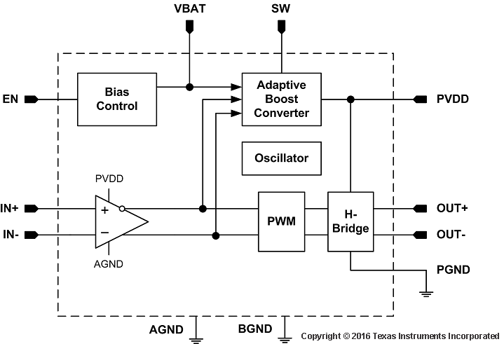
The TPA2080D1 is a high-efficiency Class-D audio power amplifier with an integrated Class-G boost converter that enhances efficiency at low output power. The built-in converter generates a 5.75-V supply voltage for the Class-D amplifier when high output power is required. The device has a integrated low-pass filter to improve the RF rejection and reduce DAC out-of-band noise, increasing the signal-to-noise ratio (SNR).
9.2 Functional Block Diagram

9.3 Feature Description
9.3.1 Fully Differential Amplifier
The TPA2080D1 is a fully differential amplifier with differential inputs and outputs. The fully differential amplifier consists of a differential amplifier with common-mode feedback. The differential amplifier ensures that the amplifier outputs a differential voltage on the output that is equal to the differential input times the gain. The common-mode feedback ensures that the common-mode voltage at the output is biased around VCC/2 regardless of the common-mode voltage at the input. The fully differential TPA2080D1 can still be used with a single-ended input; however, the TPA2080D1 must be used with differential inputs when in a noisy environment, like a wireless handset, to ensure maximum noise rejection.
9.3.1.1 Advantages of Fully Differential Amplifiers
- Input-coupling capacitors not required:
- The fully differential amplifier allows the inputs to be biased at voltage other than mid-supply. The inputs of the TPA2080D1 can be biased anywhere within the common-mode input voltage range listed in Recommended Operating Conditions and Electrical Characteristics. If the inputs are biased outside of that range, input-coupling capacitors are required.
- Midsupply bypass capacitor, C(BYPASS), not required:
- The fully differential amplifier does not require a bypass capacitor. Any shift in the midsupply affects both positive and negative channels equally and cancels at the differential output.
- Better RF-immunity:
- GSM handsets save power by turning on and shutting off the RF transmitter at a rate of 217 Hz. The transmitted signal is picked up on input and output traces. The fully differential amplifier cancels the signal better than the typical audio amplifier.
9.3.2 Short-Circuit Auto-Recovery
When a short-circuit event happens, the TPA2080D1 goes to low duty cycle mode and tries to reactivate itself every 1.6 seconds. The auto-recovery will continue until the short-circuit event stops. This feature protects the device without affecting the long-term reliability of the device.
9.3.3 Operation With DACs and CODECs
Large noise voltages can be present at the output of ΔΣ DACs and CODECs, just above the audio frequency (for example, 80 kHz with a 300 mVP-P). This out-of-band noise is due to the noise shaping of the delta-sigma modulator in the DAC. Some Class-D amplifiers have higher output noise when used in combination with these DACs and CODECs. This is because out-of-band noise from the CODEC/DAC mixes with the Class-D switching frequencies in the audio amplifier input stage. The TPA2080D1 has a built-in low-pass filter with cutoff frequency at 55 kHz that reduces the out-of-band noise and RF noise, filtering out-of-band frequencies that could degrade in-band noise performance. If driving the TPA2080D1 input with 4th-order or higher ΔΣ DACs or CODECs, add an R-C low pass filter at each of the audio inputs (IN+ and IN–) of the TPA2080D1 to ensure best performance. The recommended resistor value is 100 Ω and the capacitor value of 47 nF.
9.3.4 Speaker Load Limitation
Speakers are nonlinear loads with varying impedance (magnitude and phase) over the audio frequency. A portion of speaker load current can flow back into the boost converter output through the Class-D output H-bridge high-side device. This is dependent on the phase change over frequency on the speaker, and the audio signal amplitude and frequency content. Most portable speakers have limited phase change at the resonant frequency, typically no more than 40 or 50 degrees. To avoid excess flow-back current, use speakers with limited phase change. Otherwise, flow-back current could drive the PVDD voltage above the absolute maximum recommended operational voltage.
Confirm proper operation by connecting the speaker to the TPA2080D1 and driving it at maximum output swing. Observe the PVDD voltage with an oscilloscope. In the unlikely event the PVDD voltage exceeds 6.5 V, add a 6.8-V Zener diode between PVDD and ground to ensure the TPA2080D1 operates properly. The amplifier has thermal overload protection and deactivates if the die temperature exceeds 150°C. It automatically reactivates once die temperature returns below 150°C. Built-in output overcurrent protection deactivates the amplifier if the speaker load becomes short-circuited. The amplifier automatically restarts 1.6 seconds after the overcurrent event. Although the TPA2080D1 Class-D output can withstand a short between OUT+ and OUT–, do not connect either output directly to GND, VDD, or VBAT as this could damage the device.
9.3.5 Filter-Free Operation and Ferrite Bead Filters.
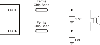
A ferrite bead filter can often be used if the design is failing radiated emissions without an LC filter and the frequency sensitive circuit is greater than 1 MHz. This filter functions well for circuits that just have to pass FCC and CE because FCC and CE only test radiated emissions greater than 30 MHz. When choosing a ferrite bead, choose one with high impedance at high frequencies, and very low impedance at low frequencies. In addition, select a ferrite bead with adequate current rating to prevent distortion of the output signal.
Use an LC output filter if there are low-frequency, (< 1 MHz) EMI-sensitive circuits or long leads from amplifier to speaker.
Figure 21 shows a typical ferrite bead output filters.
 Figure 21. Typical Ferrite Chip Bead Filter
Table 1. Suggested Chip Ferrite Bead
| LOAD | VENDOR | PART NUMBER | SIZE |
|---|---|---|---|
| 8 Ω | Murata | BLM18EG121SN1 | 0603 |
| 4 Ω | TDK | MPZ2012S101A | 0805 |
9.3.6 Boost Converter Auto Pass Through (APT)
The TPA2080D1 consists of a Class-G boost converter and a Class-D amplifier. The boost converter operates from the supply voltage, VBAT, and generates a higher output voltage PVDD at 5.75 V. PVDD drives the supply voltage of the Class-D amplifier. This improves loudness over non-boosted solutions. The boost converter has a pass through mode in which it turns off automatically and PVDD is directly connected to VBAT through an internal bypass switch.
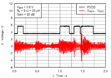
The boost converter is adaptive and operates between pass through mode and boost mode depending on the output audio signal amplitude. When the audio output amplitude exceeds the auto pass through (APT) threshold, the boost converter is activated automatically and goes to boost mode. The transition time from normal mode to boost mode is fast enough to prevent clipping large transient audio signals. The APT threshold of the TPA2080D1 is fixed at 2 VPEAK. When the audio output signal is below APT threshold, the boost converter is deactivated and goes to pass through mode. The adaptive boost converter maximizes system efficiency at lower audio output levels.
The Class-G boost converter is designed to drive the Class-D amplifier only. Do not use the boost converter to drive external devices.
Figure 22 shows how the adaptive boost converter behaves with a typical audio signal.
 Figure 22. Class-G Boost Converter With Typical Music Playback
9.4 Device Functional Modes
9.4.1 Shutdown Mode
The TPA2080D1 can be put in shutdown mode when asserting EN to a logic LOW. While in shutdown mode, the device output stage is turned off and the current consumption is very low.